US8364856B2 - Memory module with configurable input/output ports - Google Patents
Memory module with configurable input/output ports Download PDFInfo
- Publication number
- US8364856B2 US8364856B2 US13/445,083 US201213445083A US8364856B2 US 8364856 B2 US8364856 B2 US 8364856B2 US 201213445083 A US201213445083 A US 201213445083A US 8364856 B2 US8364856 B2 US 8364856B2
- Authority
- US
- United States
- Prior art keywords
- memory module
- input
- memory
- output ports
- controller
- Prior art date
- Legal status (The legal status is an assumption and is not a legal conclusion. Google has not performed a legal analysis and makes no representation as to the accuracy of the status listed.)
- Active
Links
Images


Classifications
-
- G—PHYSICS
- G11—INFORMATION STORAGE
- G11C—STATIC STORES
- G11C7/00—Arrangements for writing information into, or reading information out from, a digital store
- G11C7/10—Input/output [I/O] data interface arrangements, e.g. I/O data control circuits, I/O data buffers
- G11C7/1015—Read-write modes for single port memories, i.e. having either a random port or a serial port
- G11C7/1045—Read-write mode select circuits
-
- G—PHYSICS
- G11—INFORMATION STORAGE
- G11C—STATIC STORES
- G11C5/00—Details of stores covered by group G11C11/00
Definitions
- the present disclosure relates generally to memory modules and in particular the present disclosure relates to memory modules with configurable input/output ports.
- Memory modules such as memory cards, are commonly used in electronic devices, such as personal computers, personal digital assistants (PDAs), digital cameras, digital media players, cellular telephones.
- memory modules such as flash memory modules, may be configured as removable memory that can be removably coupled to a host device, such as a processor of an electronic device.
- a typical memory module may include one or more memory devices coupled to a memory controller.
- Each memory device may be a NAND or a NOR flash memory device, dynamic random access memory (DRAM) device, static random access memory (SRAM) device, or the like and may include an array of memory cells, such as non-volatile memory cells.
- the memory controller provides data signals, address signals, and control signals to each of the one or more memory devices.
- the memory controller is usually placed in communication with a host via an input/output interface (e.g., which is often referred to as an input/output bus) for coupling to a host device to form part of an electronic system.
- an input/output bus is a USB (Universal Serial Bus) interface.
- the input/output interface typically provides one or more data signal links (often referred to as lanes), e.g., 1, 4, 8, 16, etc., over which the controller can receive data signals from the host and/or over which the controller can send data signals to the host.
- the input/output data signal lanes may include unidirectional or bidirectional data signal lines.
- the number of input/output data signal lanes is often referred to as the input/output bus width of the input/output interface.
- conventional interfaces are limited in that the same input/output data signal lanes that are used for output are also typically used for input.
- FIG. 1 is a block-diagram illustration of an embodiment of an electronic system, according to an embodiment of the disclosure.
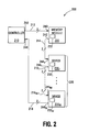
- FIG. 2 is a block-diagram illustration of an embodiment of an electronic system configured as a ring, according to another embodiment of the disclosure.
- FIG. 3 is a block-diagram illustration of another embodiment of an electronic system, according to another embodiment of the disclosure.
- FIG. 4 is a block-diagram illustration of another embodiment of an electronic system, according to another embodiment of the disclosure.
- FIG. 5 is a block-diagram illustration of another embodiment of an electronic system, according to another embodiment of the disclosure.
- FIG. 6 is a block-diagram illustration of another embodiment of an electronic system, according to another embodiment of the disclosure.
- FIG. 1 is a block-diagram illustration of a memory module 100 , such as a memory card, coupled to a host controller 110 , e.g., as part of an electronic system, according to an embodiment.
- a memory module 100 such as a memory card
- host controller 110 e.g., as part of an electronic system
- electronic systems include such systems as computer systems, peripheral devices, cellular and wireless devices, digital cameras, audio recorders, personal digital assistants (PDAs), etc.
- PDAs personal digital assistants
- memory module 100 may include one or more memory devices 120 , such as memory chips or dies, in communication with a memory controller 130 .
- memory devices include NAND, NOR, or other non-volatile memory devices, dynamic random access memory devices (DRAMs), static random access memory devices (SRAMs), or the like.
- Each memory device 120 may include an array of memory cells, such as non-volatile memory cells.
- Host controller 110 provides control signals, such as command signals (commands) and address signals (addresses), to memory controller 130 over an external control signal link 140 that is external to memory module 100 and that is coupled between host controller 110 and memory controller 130 .
- memory controller 130 may send configuration signals (configuration information), e.g., indicative of its configuration and/or the configuration of memory module 100 , to host controller 110 over control signal link 140 .
- Configuration information e.g., indicative of its configuration and/or the configuration of memory module 100
- Data signals (data) may be sent from input/output ports 142 of host controller 110 to input/output ports 144 of memory controller 130 over external data links 150 (also referred to as data lanes) during write operations.
- Data signals may be received at input/output ports 142 of host controller 110 from input/output ports 144 of memory controller 130 over data links 150 during read operations.
- Memory controller 130 provides address signals and/or command signals, e.g., in response to commands and/or addresses received from host controller 110 , to one or more of the memory devices 120 over an internal control link 160 that is internal to memory module 100 .
- Memory controller 130 also sends data received from host controller 110 , during the write operations, to one or more of the memory devices 120 over an internal data link 170 that is internal to memory module 100 .
- Memory controller 130 also receives data, during the read operations, from one or more of the memory devices 120 over data link 170 for subsequent transmission to host controller 110 .
- data link 170 may be a data bus having a bus width of 1, 2, 4, 8, 16, 32, or 64 bits, etc.
- a first number of data links 150 may be unidirectional and may be configured to convey data in a first direction, e.g., from host controller 110 to memory controller 130 , e.g., during a write operation. Configuring the input/output ports 142 of host controller 110 coupled to the first number of data links 150 as outputs and configuring the input/output ports 144 of memory controller 130 coupled to respective ones of the input/output ports 142 by the first number of data links 150 as inputs may accomplish this.
- a second (e.g., remaining) number of data links 150 may be unidirectional and be configured to convey data in a second direction opposite the first direction, e.g., from memory controller 130 to host controller 110 , e.g., during a read operation.
- Configuring the input/output ports 142 of host controller 110 coupled to the second number of data links 150 as inputs and configuring the input/output ports 144 of memory controller 130 coupled to respective ones of the input/output ports 142 by the second number of data links 150 as output ports may accomplish this.
- input/output ports 142 1 - 142 3 respectively coupled to data links 150 1 - 150 3 may be configured as output ports and input/output ports 144 1 - 144 3 respectively coupled to data links 150 1 - 150 3 may be configured as input ports, while input/output port 142 4 coupled to data link 150 4 may be configured as an input port and input/output port 144 4 coupled to data link 150 4 may be configured as an output port.
- This configures data links 150 1 - 150 3 to convey data from host controller 110 to memory controller 130 and data link 150 4 to convey data from memory controller 130 to host controller 110 .
- data links 150 1 - 150 2 may be configured to convey data from host controller 110 to memory controller 130
- data links 150 3 - 150 4 may be configured to convey data from memory controller 130 to host controller 110
- the read and write operations may occur concurrently so that data is concurrently conveyed from host controller 110 to memory controller 130 over a first number of data links 150 and from memory controller 130 to host controller 110 over a number portion of data links 150 .
- all of the data links 150 may be configured to convey data in a first direction, e.g., from host controller 110 to memory controller 130 , whereas a number (e.g., a fraction) of all of the data links 150 may be configured to convey data in a second direction opposite the first direction, e.g., from memory controller 130 to host controller 110 .
- all of the input/output ports 142 of host controller 110 are configured as outputs and all of the input/output ports 144 of memory controller 130 are configured as inputs
- a number of all of the input/output ports 142 of host controller 110 coupled to the portion of all of the data links 150 are configured as input ports and a portion all of the input/output ports 144 of memory controller 130 coupled to the portion of all of the data links 150 are configured as output ports.
- all of the data links 150 may be configured to convey data from memory controller 130 to host controller 110
- a number (e.g., a fraction) of all of the data links 150 may be configured to convey data from host controller 110 to memory controller 130 .
- one or more of data links 150 may be configured as bidirectional data links. Configuring one or more input/output ports 142 of host controller 110 as bidirectional input/outputs and configuring one or more input/output ports 144 of memory controller 130 respectively coupled to the one or more input/output ports 142 by data links 150 as bidirectional input/outputs (i.e., both an input and an output) may accomplish this.
- data may be conveyed from host controller 110 to memory controller 130 over a first number of the bidirectional data links and data may be conveyed from memory controller to host controller 110 to over a second number of the bidirectional data links concurrently.
- the configuration of data links 150 may be stored, e.g., as configuration data, in a register 180 , e.g., of memory controller 130 , e.g., during manufacture of memory module 100 . Then, upon start up of memory module 100 , for example, memory controller 130 reads register 180 and configures data links 150 according to the configuration stored in register 180 by configuring input/output ports 144 accordingly, e.g., as input ports for data writes from host controller 110 and/or output ports for data reads to host controller 110 .
- register 180 may contain a bit for each input/output port 144 indicating its configuration, i.e., configured as input or configured as output.
- memory controller 130 may send a signal to host controller 110 indicating the configuration of input/output ports 144 so that host controller 110 can configure input/output ports 142 to correspond to the configuration of input/output ports 144 .
- host controller 110 may configure the input/output ports 142 coupled to input/output ports 144 that are configured as input ports as output ports, while for data reads from memory controller 130 to host controller 110 , host controller 110 may configure the input/output ports 142 coupled to input/output ports 144 that are configured as output ports as input ports.
- data links 150 may be configured according to operational attributes of memory module 100 , such as the power consumption per input/output port 144 , power supplied to memory module 100 , the number of times memory devices 120 have been programmed and/or read, the data rate capacity per input/output port 144 , etc.
- host controller 110 may send a command to memory controller 130 indicating that data should be conveyed at a certain rate between host controller 110 and memory controller 130 . Based on the desired rate, the memory controller 130 may configure its input/output ports 144 to attain the desired rate.
- memory controller 130 may send its attributes to host controller 110 in response to the command, and host controller 110 may determine the number of data links 150 to be configured for conveying the data based on the attributes of memory module 100 .
- host controller 110 may configure its input/output ports 142 accordingly and may instruct memory controller 130 to configure its input/output ports 144 as input ports if coupled to an input/output port 142 configured as an output port and to configure its input/output ports 144 as output ports if coupled to an input/output port 142 configured as an input port.
- the attributes of memory module 100 may be stored in a register, such as register 180 of memory controller 130 .
- data links 150 may be configured “on the fly,” e.g., in response to commands from host controller 110 .
- host controller 110 may send a command to memory controller 130 indicating that data should be conveyed between host controller 110 and memory controller 130 at a certain overall data rate.
- Memory controller 130 may then determine how many data links 150 to use convey the data between host controller 110 and memory controller 130 based on that rate.
- the number of data links 150 may be determined from the overall data rate and an attribute of memory module 100 , such as the data rate per link, power consumption per link, power supplied to memory module 100 , etc.
- memory controller 130 may have a look-up table 185 that outputs a number of data links 150 to be used to convey the data in response to inputting the overall data rate.
- Memory controller 130 may then configure its input/output ports 144 accordingly and send an indication of the configuration of input/output ports 144 to host controller 110 so that host controller 110 can configure its input/output ports 142 to correspond to the configuration input/output ports 144 , e.g. so that input/output ports 142 that are configured as output ports are coupled to input/output ports 144 that are configured as input ports or vice versa.
- memory controller 130 may send one or more attributes of memory module 100 to host controller 110 , e.g., in response to host controller 110 's command indicating that data should be conveyed between the memory controller 130 and host controller 110 at a certain rate.
- Host controller 110 may then determine, from the one or more attributes of memory module 100 received from memory controller 130 , the number of data links 150 that may be needed to convey the data between host controller 110 and memory controller 130 at the certain rate.
- Host controller 110 may then configure that number of data links 150 by accordingly configuring that number of its input/outputs 142 for input or output and by instructing memory controller 130 to accordingly configure that number of its input/outputs 144 for input or output so that input/outputs 142 configured for output are coupled input/outputs 144 configured for input or vice versa.
- the data rate for a read operation may be less than the data rate for a write operation, where data is conveyed from host controller 110 to memory controller 130 or vice versa. Therefore, a larger number of data links 150 may be used for the write operation than the read operation or vice versa.
- the number of data links 150 to be used to convey data to or from memory controller 130 may depend on an attribute, such as the power requirements of each line of memory module 100 .
- the memory module 100 could operate at multiple power consumption levels by limiting the number of data links 150 to be used for convey data.
- the memory module 100 could configure its input/output ports 144 to maintain the power consumption below some desired level. Because power consumption will generally differ between when an input/output port 144 is used for data input and when it is used for data output, the number of input/output ports 144 designated for input need not be the same as the number designated for output.
- power consumption information such as the power consumption per data link 150 , may be stored in a register, such as register 180 of memory controller 130 , e.g., during manufacture of memory module 100 .
- memory controller 130 may be configured to configure data links 150 in response to an attribute, such as the power supplied to memory module 100 .
- an attribute such as the power supplied to memory module 100 .
- memory module 100 when memory module 100 is operating in a first power mode, e.g., memory module 100 is powered by a high-power source, such as a public power grid, a larger number of data links may be used to convey data between host controller 110 and memory controller 130 than when memory module 100 is operating in a second power mode, e.g., memory module 100 is powered by a low-power source, such as a battery.
- all of data links 150 may be used for conveying data when memory module 100 is powered by the high-power source and less than all of data links 150 may be used for conveying data when memory module 100 is powered by the low-power source.
- memory controller 130 may configure all of its input/output ports 144 as inputs or outputs and may subsequently send a signal to host controller 110 , indicating the configuration of input/output ports 144 .
- Host controller 110 may then configure all its input/output ports 142 for input or output in response to the signal so that the input/output ports 142 configured for output are respectively coupled to the input/output ports 144 configured for input or vice versa.
- memory controller 130 may configure less than all of its input/output ports 144 as input or output ports and prevent the use of (e.g., disable) the remaining input/output ports 144 .
- Memory controller 130 may then send a signal to host controller 110 , indicating the configuration of input/output ports 144 .
- Host controller 110 may then configure less than all of its input/output ports 142 (e.g., the same number input/output ports 142 and 144 will be configured) for input or output in response to the signal so that the input/output ports 142 configured for output are respectively coupled to the input/output ports 144 configured for input or vice versa.
- host controller 110 may prevent the use of (e.g., disable) the remaining input/output ports 142 that are respectively coupled to the disabled input/output ports 144 .
- the number of data links 150 used for conveying data from host controller 110 to memory controller 130 , may be based on the relative number of programming operations and read operations that have been performed on memory devices 120 . Therefore, memory controller 130 may keep track of the number of programming and read operations, and configure its input/output ports 144 so that the number of ports configured as inputs is proportional to the number of write operations and the number of ports configured as outputs is proportional to the number of read operations.
- FIG. 2 is a block diagram illustration of an electronic system 200 configured as a ring network, according to another embodiment.
- ring network 200 includes a controller 210 , such as a host controller, coupled serially, point-to-point, by a unidirectional data link 212 , to a memory module 220 that may be substantially similar to the memory module 100 described above.
- memory module 220 is coupled serially, point-to-point, to a first device (device 230 1 ) of a string 225 of devices 230 by a unidirectional data link 214 .
- the devices 230 are serially coupled, point-to-point, to each other by unidirectional data links 216 to form string 225 .
- a last device (device 230 M ) of string 225 is serially coupled, point-to-point, to controller 210 by a data link 218 to complete ring network 200 .
- each data link may have one or more lines.
- each of devices 230 may be a memory module similar to memory module 220 , a hard drive, a camera, a slave controller, etc.
- memory module 220 includes a controller 222 , e.g., similar to memory controller 130 described above, and each of devices 230 includes a controller 232 , e.g., similar to memory controller 130 .
- controller 222 of memory module 220 is configured to configure input/output ports 240 of memory module 220 as inputs and input/output ports 242 of memory module 220 as outputs.
- the controller 232 of each of devices 230 is configured to configure input/output ports 244 of that device as inputs and input/output ports 246 of that device as outputs.
- Controller 210 is configured so that its input/output ports 248 are configured as inputs and its input/output ports 250 are configured as outputs.
- memory module 220 and devices 230 are configured to operate in a pass-through mode, so that data can be passed around ring 200 .
- controller 210 may send a signal to controller 222 that instructs controller 222 to configure the input/output ports of memory module 220 in a certain way.
- the signal may be sent to the controllers 232 of devices 230 for instructing controllers 232 to configure the input/output ports of the respective devices 230 in a certain way.
- Controller 222 of memory module 220 may also be configured to determine whether data received thereat from host controller 210 is intended for memory module 220 and should be acted on by controller 222 or that the data is not intended for memory module 220 and should be passed on to device 230 1 .
- the controller 232 of each device 230 may be configured to determine whether data received thereat is intended for that device 230 and should be acted on by that controller 232 or that the data is not intended for that device 230 and should be passed on to another device 230 or to controller 210 in the case of device 230 M .
- controller 210 all of the data sent by controller 210 is passed around ring 200 and is received at memory module 220 and each of devices 230 . If controller 222 of memory module 220 determines that the data is intended for memory module 220 , then controller 222 acts on the data and/or if a controller 232 a device 230 determines that the data is intended for that device 230 , then that controller 232 acts on the data.
- FIGS. 3-5 provide examples of how a memory module 320 might configure a fixed number, e.g., four, of data input/output ports 350 , according to other embodiments.
- each of input/output ports 350 is configured for bidirectional communication with a respective one of controllers 310 .
- a bidirectional data link 340 is coupled between each input/output port 350 a respective one of controllers 310 .
- Each of controllers 310 may be host controller similar to host controller 110 , discussed above in conjunction with FIG. 1 .
- Memory module 320 may be similar to memory module 100 , discussed above in conjunction with FIG. 1 .
- the controller 330 is configured to output data and configuration signals to a controller 310 from which the corresponding access command was received.
- each of input/output ports 350 is configured for unidirectional communication.
- input/output ports 350 1 and 350 3 are configured as inputs for respectively receiving data from controllers 310 1 and 310 2 over unidirectional data links 440 1 and 440 3
- input/output ports 350 2 and 350 4 are configured as outputs for respectively sending data to controllers 310 1 and 310 2 over unidirectional data links 440 2 and 440 4 .
- the controller 330 is configured to output data and configuration signals to a controller 310 from which the corresponding access command was received. For example, if a read request is received from controller 310 1 on data link 440 1 , then data in response to that read request would be output to input/output port 350 2 . Similarly, if a write command is received from controller 310 2 on data link 440 3 , then status signals in response to that write command would be output to input/output port 350 4 .
- each of input/output ports 350 is configured for bidirectional communication.
- input/output ports 350 1 and 350 2 are configured for bidirectional communication with controller 310 1 over bidirectional data links 540 1
- input/output ports 350 3 and 350 4 are configured for bidirectional communication with controller 310 2 over bidirectional data links 540 2 .
- the controller 330 is configured to output data and configuration signals to a controller 310 from which the corresponding access command was received. For example, if a read request is received from controller 310 1 on data link 540 1 , then data in response to that read request would be output to data link 540 1 . Similarly, if a write command is received from controller 310 2 on data link 540 2 , then configuration signals in response to that write command would be output to data link 540 2 .
- a memory controller 330 of memory module 320 configures each of input/output ports 350 according to the example configurations of FIGS. 3-5 .
- one of controllers 310 e.g., controller 310 1
- controller 310 1 may temporarily act as a master controller that instructs memory controller 330 to configure each of input/output ports 350 .
- controller 310 1 may also instruct memory controller 330 to partition memory module 320 so that each memory partition corresponds to a respective one of controllers 310 .
- memory module 320 may have registers that can be read by memory controller 330 upon power up of memory module 320 and that instruct controller 330 to configure input/output ports 350 and optionally partition memory module 320 .
- FIG. 6 is a block diagram illustration of an electronic system 600 , e.g., configured as a “chain” network.
- electronic system 600 includes a controller 610 , such as a host controller, coupled serially, point-to-point, by unidirectional data links 612 and 613 , to a memory module 620 that may be substantially similar to the memory module 100 described above.
- memory module 620 is coupled serially, point-to-point, to a first device (device 630 1 ) of a string (e.g., a “chain”) 625 of devices 630 by a unidirectional data link 614 and a unidirectional data link 615 .
- the devices 630 are serially coupled, point-to-point, to each other by unidirectional data links 616 and unidirectional data links 618 to form string 625 such that each of the devices 630 forms a “link” in the “chain.”
- each data link may have one or more lines.
- each of devices 630 may be a memory module similar to memory module 620 , a hard drive, a camera, a slave controller, etc.
- memory module 620 includes a controller 622 , e.g., similar to memory controller 130 described above, and each of devices 630 includes a controller 632 , e.g., similar to memory controller 130 .
- controller 622 of memory module 620 is configured to configure input/output ports 640 of memory module 620 as inputs, input/output ports 645 of memory module 620 as outputs, and input/output ports 642 of memory module 620 as outputs.
- the controller 632 of each of devices 630 is configured to configure input/output ports 644 of that device as inputs and input/output ports 646 of that device as outputs.
- the controller 632 of each of devices 630 e.g., except the last device (device 630 K ) (e.g., devices 630 1 and 630 2 ) is configured to configure input/output ports 650 of that device as inputs and input/output ports 652 of that device as outputs.
- Controller 610 is configured so that its input/output ports 660 are configured as inputs and its input/output ports 662 are configured as outputs.
- memory module 620 and devices 630 can be configured to operate in a pass-through mode so that data can be passed from controller 610 to device 630 K through memory module 620 and through the successive devices 630 (e.g., devices 630 1 and 630 2 in succession). Data may be passed to controller 610 from device 630 K through the successive devices 630 (e.g., devices 630 2 and 630 1 in succession).
- data do not need to pass through subsequent devices 630 before being returned to controller 610 , as indicated by dashed arrow 670 of memory module 620 and dashed arrows 672 of devices 630 .
- data received at input 640 of memory module 620 from controller 610 may be returned to controller 610 through output 645 of memory module 620 without passing through any of devices 630 , as indicated by dashed arrow 670 .
- data received at input 644 of device 630 1 from memory module 620 may be returned to controller 610 through output 652 of device 630 1 by passing through memory module 620 and without passing through any of the remaining devices 630 downstream of device 630 1 (e.g., devices 630 2 and 630 K ), in a direction from controller 610 , as indicated by dashed arrow 672 of device 630 1 .
- data received at input 644 of device 630 2 from device 630 1 may be returned to controller 610 through output 652 of device 630 2 by passing through device 630 1 and memory module 620 and without passing through any of the remaining devices 630 downstream of device 630 2 (e.g., device 630 K ), as indicated by dashed arrow 672 of device 630 2 .
- controller 610 may send a signal to controller 622 that instructs controller 622 to configure the input/output ports of memory module 620 in a certain way.
- the signal may be sent to the controllers 632 of devices 630 for instructing controllers 632 to configure the input/output ports of the respective devices 630 in a certain way.
- a device 630 located upstream (e.g., in a direction toward controller 110 ) of a downstream device 630 (e.g., device 630 2 ) may configure the downstream device 630 in a certain way or vice versa, e.g., downstream device 630 2 may configure upstream device 630 1 .
- Controller 622 of memory module 620 may also be configured to determine whether data received thereat from host controller 610 and intended for memory module 620 and should be acted on by controller 622 or that data is not intended for memory module 620 and should be passed on to device 630 1 .
- the controller 632 of each device 630 may be configured to determine whether data received thereat is intended for that device 630 and should be acted on by that controller 632 or that the data is not intended for that device 630 and should be passed on to another device 630 or to controller 610 .
- all of the data sent by controller 610 can be passed along the chain and can be received at memory module 620 and each of devices 630 . If controller 622 of memory module 620 determines that the data is intended for memory module 620 , then controller 622 acts on the data and/or if a controller 632 of a device 630 determines that the data is intended for that device 630 , then that controller 632 acts on the data.
- memory module 620 and each of devices 630 can perform different operations concurrently.
- memory module 620 or a device 630 can receive and act on data moving in a direction (e.g., downstream) from controller 610 and can independently and concurrently receive and act on data moving in an opposite direction (e.g., upstream) toward controller 610 .
- the memory module 620 and each of devices 630 may be configured to operate at different rates.
Abstract
Description
Claims (32)
Priority Applications (1)
| Application Number | Priority Date | Filing Date | Title |
|---|---|---|---|
| US13/445,083 US8364856B2 (en) | 2008-05-05 | 2012-04-12 | Memory module with configurable input/output ports |
Applications Claiming Priority (2)
| Application Number | Priority Date | Filing Date | Title |
|---|---|---|---|
| US12/115,047 US8171181B2 (en) | 2008-05-05 | 2008-05-05 | Memory module with configurable input/output ports |
| US13/445,083 US8364856B2 (en) | 2008-05-05 | 2012-04-12 | Memory module with configurable input/output ports |
Related Parent Applications (1)
| Application Number | Title | Priority Date | Filing Date |
|---|---|---|---|
| US12/115,047 Continuation US8171181B2 (en) | 2008-05-05 | 2008-05-05 | Memory module with configurable input/output ports |
Publications (2)
| Publication Number | Publication Date |
|---|---|
| US20120198201A1 US20120198201A1 (en) | 2012-08-02 |
| US8364856B2 true US8364856B2 (en) | 2013-01-29 |
Family
ID=41257864
Family Applications (2)
| Application Number | Title | Priority Date | Filing Date |
|---|---|---|---|
| US12/115,047 Active 2028-10-02 US8171181B2 (en) | 2008-05-05 | 2008-05-05 | Memory module with configurable input/output ports |
| US13/445,083 Active US8364856B2 (en) | 2008-05-05 | 2012-04-12 | Memory module with configurable input/output ports |
Family Applications Before (1)
| Application Number | Title | Priority Date | Filing Date |
|---|---|---|---|
| US12/115,047 Active 2028-10-02 US8171181B2 (en) | 2008-05-05 | 2008-05-05 | Memory module with configurable input/output ports |
Country Status (7)
| Country | Link |
|---|---|
| US (2) | US8171181B2 (en) |
| EP (2) | EP2743928B1 (en) |
| JP (2) | JP5093401B2 (en) |
| KR (1) | KR101221265B1 (en) |
| CN (1) | CN102017002A (en) |
| TW (1) | TWI413128B (en) |
| WO (1) | WO2009137459A2 (en) |
Families Citing this family (8)
| Publication number | Priority date | Publication date | Assignee | Title |
|---|---|---|---|---|
| US7948821B2 (en) | 2008-12-15 | 2011-05-24 | Micron Technology, Inc. | Reduced signal interface memory device, system, and method |
| WO2010093529A2 (en) * | 2009-02-12 | 2010-08-19 | Rambus Inc. | Memory interface with reduced read-write turnaround delay |
| US8832354B2 (en) * | 2009-03-25 | 2014-09-09 | Apple Inc. | Use of host system resources by memory controller |
| US8769213B2 (en) | 2009-08-24 | 2014-07-01 | Micron Technology, Inc. | Multi-port memory and operation |
| US8429391B2 (en) | 2010-04-16 | 2013-04-23 | Micron Technology, Inc. | Boot partitions in memory devices and systems |
| US8380940B2 (en) * | 2010-06-25 | 2013-02-19 | Qualcomm Incorporated | Multi-channel multi-port memory |
| US9602101B2 (en) * | 2013-10-07 | 2017-03-21 | Microchip Technology Incorporated | Integrated device with auto configuration |
| CN113868167A (en) * | 2020-06-30 | 2021-12-31 | 华为技术有限公司 | Chip module, communication system and port distribution method |
Citations (13)
| Publication number | Priority date | Publication date | Assignee | Title |
|---|---|---|---|---|
| US6067318A (en) | 1994-09-02 | 2000-05-23 | Microcom Systems, Inc. | High performance communications interface |
| US20020087751A1 (en) | 1999-03-04 | 2002-07-04 | Advanced Micro Devices, Inc. | Switch based scalable preformance storage architecture |
| US20020112119A1 (en) | 1998-02-13 | 2002-08-15 | Intel Corporation | Dual-port buffer-to-memory interface |
| US20050271078A1 (en) | 2004-06-01 | 2005-12-08 | Quayle Barton L | System and method for configuring communication systems |
| US20060184809A1 (en) | 2005-02-10 | 2006-08-17 | Akihiro Kojou | Information processing apparatus and control method for the same |
| US20070124532A1 (en) | 2005-04-21 | 2007-05-31 | Bennett Jon C | Interconnection system |
| US20070300201A1 (en) | 2006-06-23 | 2007-12-27 | National Inst Of Adv Industrial Science And Tech. | System for configuring an integrated circuit and method thereof |
| US7406572B1 (en) | 2004-03-26 | 2008-07-29 | Cypress Semiconductor Corp. | Universal memory circuit architecture supporting multiple memory interface options |
| US20080276020A1 (en) | 2004-01-28 | 2008-11-06 | Rambus Inc. | Adaptive-Allocation Of I/O Bandwidth Using A Configurable Interconnect Topology |
| US20090187680A1 (en) | 2008-01-21 | 2009-07-23 | Shih-Chieh Liao | Controller System With Programmable Bi-directional Terminals |
| US7610500B2 (en) | 2004-05-21 | 2009-10-27 | Intel Corporation | Link power saving state |
| US7788439B1 (en) | 2003-05-07 | 2010-08-31 | Nvidia Corporation | Asymmetrical bus for bus link width optimization of a graphics system |
| US20120030386A1 (en) * | 2003-10-30 | 2012-02-02 | International Business Machines Corporation | Configurable Interface Controller |
Family Cites Families (14)
| Publication number | Priority date | Publication date | Assignee | Title |
|---|---|---|---|---|
| JP2684793B2 (en) * | 1989-10-24 | 1997-12-03 | 松下電器産業株式会社 | Information processing device |
| JPH05181609A (en) * | 1992-01-06 | 1993-07-23 | Nec Corp | Personal computer system |
| JP3946873B2 (en) * | 1998-06-19 | 2007-07-18 | 株式会社日立製作所 | Disk array controller |
| JP2001067306A (en) * | 1999-08-26 | 2001-03-16 | Matsushita Electric Ind Co Ltd | Bus interface device and data transfer device |
| JP2002229848A (en) * | 2001-02-05 | 2002-08-16 | Hitachi Ltd | Processor system equipped with shared memory |
| JP2002259327A (en) * | 2001-02-28 | 2002-09-13 | Hitachi Ltd | Bus control circuit |
| TW594486B (en) * | 2002-12-30 | 2004-06-21 | Icp Electronics Inc | The improvement to the 4-wire/3-wire NVRAM control instruction |
| JP2005025473A (en) * | 2003-07-01 | 2005-01-27 | Matsushita Electric Ind Co Ltd | Composite input and output device |
| JP4928715B2 (en) * | 2004-05-07 | 2012-05-09 | 株式会社リコー | Serial data transfer device, image output device, image input device, and image forming device |
| US8046488B2 (en) | 2004-05-21 | 2011-10-25 | Intel Corporation | Dynamically modulating link width |
| US8151030B2 (en) * | 2004-05-26 | 2012-04-03 | Ocz Technology Group, Inc. | Method of increasing DDR memory bandwidth in DDR SDRAM modules |
| US7506343B2 (en) * | 2004-08-19 | 2009-03-17 | International Business Machines Corporation | System and method for passing information from one device driver to another |
| TWI260069B (en) * | 2004-08-24 | 2006-08-11 | Chipmos Technologies Inc | Memory module and method for manufacturing the same |
| US20060203559A1 (en) * | 2005-02-28 | 2006-09-14 | Peter Poechmueller | Memory device with customizable configuration |
-
2008
- 2008-05-05 US US12/115,047 patent/US8171181B2/en active Active
-
2009
- 2009-05-05 EP EP14000755.0A patent/EP2743928B1/en active Active
- 2009-05-05 CN CN2009801160984A patent/CN102017002A/en active Pending
- 2009-05-05 WO PCT/US2009/042813 patent/WO2009137459A2/en active Application Filing
- 2009-05-05 EP EP09743445.0A patent/EP2272066B1/en active Active
- 2009-05-05 TW TW098114842A patent/TWI413128B/en not_active IP Right Cessation
- 2009-05-05 JP JP2011507716A patent/JP5093401B2/en active Active
- 2009-05-05 KR KR1020107027203A patent/KR101221265B1/en active IP Right Grant
-
2012
- 2012-04-12 US US13/445,083 patent/US8364856B2/en active Active
- 2012-09-03 JP JP2012192733A patent/JP5533963B2/en active Active
Patent Citations (13)
| Publication number | Priority date | Publication date | Assignee | Title |
|---|---|---|---|---|
| US6067318A (en) | 1994-09-02 | 2000-05-23 | Microcom Systems, Inc. | High performance communications interface |
| US20020112119A1 (en) | 1998-02-13 | 2002-08-15 | Intel Corporation | Dual-port buffer-to-memory interface |
| US20020087751A1 (en) | 1999-03-04 | 2002-07-04 | Advanced Micro Devices, Inc. | Switch based scalable preformance storage architecture |
| US7788439B1 (en) | 2003-05-07 | 2010-08-31 | Nvidia Corporation | Asymmetrical bus for bus link width optimization of a graphics system |
| US20120030386A1 (en) * | 2003-10-30 | 2012-02-02 | International Business Machines Corporation | Configurable Interface Controller |
| US20080276020A1 (en) | 2004-01-28 | 2008-11-06 | Rambus Inc. | Adaptive-Allocation Of I/O Bandwidth Using A Configurable Interconnect Topology |
| US7406572B1 (en) | 2004-03-26 | 2008-07-29 | Cypress Semiconductor Corp. | Universal memory circuit architecture supporting multiple memory interface options |
| US7610500B2 (en) | 2004-05-21 | 2009-10-27 | Intel Corporation | Link power saving state |
| US20050271078A1 (en) | 2004-06-01 | 2005-12-08 | Quayle Barton L | System and method for configuring communication systems |
| US20060184809A1 (en) | 2005-02-10 | 2006-08-17 | Akihiro Kojou | Information processing apparatus and control method for the same |
| US20070124532A1 (en) | 2005-04-21 | 2007-05-31 | Bennett Jon C | Interconnection system |
| US20070300201A1 (en) | 2006-06-23 | 2007-12-27 | National Inst Of Adv Industrial Science And Tech. | System for configuring an integrated circuit and method thereof |
| US20090187680A1 (en) | 2008-01-21 | 2009-07-23 | Shih-Chieh Liao | Controller System With Programmable Bi-directional Terminals |
Also Published As
| Publication number | Publication date |
|---|---|
| EP2743928B1 (en) | 2017-02-15 |
| EP2272066A2 (en) | 2011-01-12 |
| JP2011520192A (en) | 2011-07-14 |
| JP5093401B2 (en) | 2012-12-12 |
| US8171181B2 (en) | 2012-05-01 |
| US20120198201A1 (en) | 2012-08-02 |
| WO2009137459A3 (en) | 2010-02-18 |
| KR101221265B1 (en) | 2013-01-11 |
| WO2009137459A2 (en) | 2009-11-12 |
| EP2272066B1 (en) | 2014-06-18 |
| KR20110004895A (en) | 2011-01-14 |
| CN102017002A (en) | 2011-04-13 |
| JP2013047952A (en) | 2013-03-07 |
| TWI413128B (en) | 2013-10-21 |
| JP5533963B2 (en) | 2014-06-25 |
| EP2272066A4 (en) | 2011-06-08 |
| TW200949852A (en) | 2009-12-01 |
| US20090276545A1 (en) | 2009-11-05 |
| EP2743928A1 (en) | 2014-06-18 |
Similar Documents
| Publication | Publication Date | Title |
|---|---|---|
| US8364856B2 (en) | Memory module with configurable input/output ports | |
| US11886754B2 (en) | Apparatuses and methods for configuring I/Os of memory for hybrid memory modules | |
| TWI453760B (en) | Daisy chain cascade configuration recognition technique | |
| US20230251794A1 (en) | Buffer circuit with data bit inversion | |
| US7721130B2 (en) | Apparatus and method for switching an apparatus to a power saving mode | |
| TWI467382B (en) | Data writing method for non-volatile memory and controller and storage system using the same | |
| US10191692B2 (en) | Memory device and method of operating the same | |
| US11436167B2 (en) | Interface components between a controller and memory devices | |
| US10032494B2 (en) | Data processing systems and a plurality of memory modules | |
| EP3049942B1 (en) | Mapping memory controller connectors to memory connectors | |
| TWI688864B (en) | Storage apparatus and storing method | |
| US7702859B2 (en) | Detachable direct memory access arrangement |
Legal Events
| Date | Code | Title | Description |
|---|---|---|---|
| FEPP | Fee payment procedure |
Free format text: PAYOR NUMBER ASSIGNED (ORIGINAL EVENT CODE: ASPN); ENTITY STATUS OF PATENT OWNER: LARGE ENTITY |
|
| STCF | Information on status: patent grant |
Free format text: PATENTED CASE |
|
| CC | Certificate of correction | ||
| AS | Assignment |
Owner name: U.S. BANK NATIONAL ASSOCIATION, AS COLLATERAL AGENT, CALIFORNIA Free format text: SECURITY INTEREST;ASSIGNOR:MICRON TECHNOLOGY, INC.;REEL/FRAME:038669/0001 Effective date: 20160426 Owner name: U.S. BANK NATIONAL ASSOCIATION, AS COLLATERAL AGEN Free format text: SECURITY INTEREST;ASSIGNOR:MICRON TECHNOLOGY, INC.;REEL/FRAME:038669/0001 Effective date: 20160426 |
|
| AS | Assignment |
Owner name: MORGAN STANLEY SENIOR FUNDING, INC., AS COLLATERAL AGENT, MARYLAND Free format text: PATENT SECURITY AGREEMENT;ASSIGNOR:MICRON TECHNOLOGY, INC.;REEL/FRAME:038954/0001 Effective date: 20160426 Owner name: MORGAN STANLEY SENIOR FUNDING, INC., AS COLLATERAL Free format text: PATENT SECURITY AGREEMENT;ASSIGNOR:MICRON TECHNOLOGY, INC.;REEL/FRAME:038954/0001 Effective date: 20160426 |
|
| FPAY | Fee payment |
Year of fee payment: 4 |
|
| AS | Assignment |
Owner name: U.S. BANK NATIONAL ASSOCIATION, AS COLLATERAL AGENT, CALIFORNIA Free format text: CORRECTIVE ASSIGNMENT TO CORRECT THE REPLACE ERRONEOUSLY FILED PATENT #7358718 WITH THE CORRECT PATENT #7358178 PREVIOUSLY RECORDED ON REEL 038669 FRAME 0001. ASSIGNOR(S) HEREBY CONFIRMS THE SECURITY INTEREST;ASSIGNOR:MICRON TECHNOLOGY, INC.;REEL/FRAME:043079/0001 Effective date: 20160426 Owner name: U.S. BANK NATIONAL ASSOCIATION, AS COLLATERAL AGEN Free format text: CORRECTIVE ASSIGNMENT TO CORRECT THE REPLACE ERRONEOUSLY FILED PATENT #7358718 WITH THE CORRECT PATENT #7358178 PREVIOUSLY RECORDED ON REEL 038669 FRAME 0001. ASSIGNOR(S) HEREBY CONFIRMS THE SECURITY INTEREST;ASSIGNOR:MICRON TECHNOLOGY, INC.;REEL/FRAME:043079/0001 Effective date: 20160426 |
|
| AS | Assignment |
Owner name: JPMORGAN CHASE BANK, N.A., AS COLLATERAL AGENT, ILLINOIS Free format text: SECURITY INTEREST;ASSIGNORS:MICRON TECHNOLOGY, INC.;MICRON SEMICONDUCTOR PRODUCTS, INC.;REEL/FRAME:047540/0001 Effective date: 20180703 Owner name: JPMORGAN CHASE BANK, N.A., AS COLLATERAL AGENT, IL Free format text: SECURITY INTEREST;ASSIGNORS:MICRON TECHNOLOGY, INC.;MICRON SEMICONDUCTOR PRODUCTS, INC.;REEL/FRAME:047540/0001 Effective date: 20180703 |
|
| AS | Assignment |
Owner name: MICRON TECHNOLOGY, INC., IDAHO Free format text: RELEASE BY SECURED PARTY;ASSIGNOR:U.S. BANK NATIONAL ASSOCIATION, AS COLLATERAL AGENT;REEL/FRAME:047243/0001 Effective date: 20180629 |
|
| AS | Assignment |
Owner name: MICRON TECHNOLOGY, INC., IDAHO Free format text: RELEASE BY SECURED PARTY;ASSIGNOR:MORGAN STANLEY SENIOR FUNDING, INC., AS COLLATERAL AGENT;REEL/FRAME:050937/0001 Effective date: 20190731 |
|
| AS | Assignment |
Owner name: MICRON SEMICONDUCTOR PRODUCTS, INC., IDAHO Free format text: RELEASE BY SECURED PARTY;ASSIGNOR:JPMORGAN CHASE BANK, N.A., AS COLLATERAL AGENT;REEL/FRAME:051028/0001 Effective date: 20190731 Owner name: MICRON TECHNOLOGY, INC., IDAHO Free format text: RELEASE BY SECURED PARTY;ASSIGNOR:JPMORGAN CHASE BANK, N.A., AS COLLATERAL AGENT;REEL/FRAME:051028/0001 Effective date: 20190731 |
|
| MAFP | Maintenance fee payment |
Free format text: PAYMENT OF MAINTENANCE FEE, 8TH YEAR, LARGE ENTITY (ORIGINAL EVENT CODE: M1552); ENTITY STATUS OF PATENT OWNER: LARGE ENTITY Year of fee payment: 8 |