US6247124B1 - Branch prediction entry with target line index calculated using relative position of second operation of two step branch operation in a line of instructions - Google Patents
Branch prediction entry with target line index calculated using relative position of second operation of two step branch operation in a line of instructions Download PDFInfo
- Publication number
- US6247124B1 US6247124B1 US09/363,635 US36363599A US6247124B1 US 6247124 B1 US6247124 B1 US 6247124B1 US 36363599 A US36363599 A US 36363599A US 6247124 B1 US6247124 B1 US 6247124B1
- Authority
- US
- United States
- Prior art keywords
- branch
- instruction
- instructions
- line
- target
- Prior art date
- Legal status (The legal status is an assumption and is not a legal conclusion. Google has not performed a legal analysis and makes no representation as to the accuracy of the status listed.)
- Expired - Lifetime
Links
- 238000000034 method Methods 0.000 claims description 10
- 238000012545 processing Methods 0.000 claims description 8
- 230000008859 change Effects 0.000 claims description 2
- 238000004891 communication Methods 0.000 description 68
- 238000010586 diagram Methods 0.000 description 20
- 239000000872 buffer Substances 0.000 description 18
- 230000004044 response Effects 0.000 description 4
- 238000012937 correction Methods 0.000 description 2
- 230000006870 function Effects 0.000 description 2
- 230000004048 modification Effects 0.000 description 2
- 238000012986 modification Methods 0.000 description 2
- 238000010276 construction Methods 0.000 description 1
- 230000003111 delayed effect Effects 0.000 description 1
- 238000007689 inspection Methods 0.000 description 1
- 230000008569 process Effects 0.000 description 1
- 230000000717 retained effect Effects 0.000 description 1
Images


Classifications
-
- G—PHYSICS
- G06—COMPUTING; CALCULATING OR COUNTING
- G06F—ELECTRIC DIGITAL DATA PROCESSING
- G06F9/00—Arrangements for program control, e.g. control units
- G06F9/06—Arrangements for program control, e.g. control units using stored programs, i.e. using an internal store of processing equipment to receive or retain programs
- G06F9/30—Arrangements for executing machine instructions, e.g. instruction decode
- G06F9/38—Concurrent instruction execution, e.g. pipeline, look ahead
- G06F9/3885—Concurrent instruction execution, e.g. pipeline, look ahead using a plurality of independent parallel functional units
-
- G—PHYSICS
- G06—COMPUTING; CALCULATING OR COUNTING
- G06F—ELECTRIC DIGITAL DATA PROCESSING
- G06F9/00—Arrangements for program control, e.g. control units
- G06F9/06—Arrangements for program control, e.g. control units using stored programs, i.e. using an internal store of processing equipment to receive or retain programs
- G06F9/30—Arrangements for executing machine instructions, e.g. instruction decode
- G06F9/32—Address formation of the next instruction, e.g. by incrementing the instruction counter
- G06F9/322—Address formation of the next instruction, e.g. by incrementing the instruction counter for non-sequential address
-
- G—PHYSICS
- G06—COMPUTING; CALCULATING OR COUNTING
- G06F—ELECTRIC DIGITAL DATA PROCESSING
- G06F9/00—Arrangements for program control, e.g. control units
- G06F9/06—Arrangements for program control, e.g. control units using stored programs, i.e. using an internal store of processing equipment to receive or retain programs
- G06F9/30—Arrangements for executing machine instructions, e.g. instruction decode
- G06F9/38—Concurrent instruction execution, e.g. pipeline, look ahead
- G06F9/3802—Instruction prefetching
- G06F9/3804—Instruction prefetching for branches, e.g. hedging, branch folding
- G06F9/3806—Instruction prefetching for branches, e.g. hedging, branch folding using address prediction, e.g. return stack, branch history buffer
-
- G—PHYSICS
- G06—COMPUTING; CALCULATING OR COUNTING
- G06F—ELECTRIC DIGITAL DATA PROCESSING
- G06F9/00—Arrangements for program control, e.g. control units
- G06F9/06—Arrangements for program control, e.g. control units using stored programs, i.e. using an internal store of processing equipment to receive or retain programs
- G06F9/30—Arrangements for executing machine instructions, e.g. instruction decode
- G06F9/38—Concurrent instruction execution, e.g. pipeline, look ahead
- G06F9/3802—Instruction prefetching
- G06F9/3814—Implementation provisions of instruction buffers, e.g. prefetch buffer; banks
-
- G—PHYSICS
- G06—COMPUTING; CALCULATING OR COUNTING
- G06F—ELECTRIC DIGITAL DATA PROCESSING
- G06F9/00—Arrangements for program control, e.g. control units
- G06F9/06—Arrangements for program control, e.g. control units using stored programs, i.e. using an internal store of processing equipment to receive or retain programs
- G06F9/30—Arrangements for executing machine instructions, e.g. instruction decode
- G06F9/38—Concurrent instruction execution, e.g. pipeline, look ahead
- G06F9/3836—Instruction issuing, e.g. dynamic instruction scheduling or out of order instruction execution
- G06F9/3842—Speculative instruction execution
- G06F9/3844—Speculative instruction execution using dynamic branch prediction, e.g. using branch history tables
Definitions
- This invention relates to computing systems and, more particularly, to an apparatus for processing instructions in a computing system.
- FIGS. 1A-1C show a conventional system where up to four instructions may be executed at a time. Assume the instructions are alphabetically listed in program sequence.
- an instruction buffer 10 contains a plurality of lines 14 A-C of instructions, wherein each line contains four instructions.
- the instructions stored in buffer 10 are loaded into a dispatch register 18 , comprising four registers 22 A-D, before they are dispatched for execution. When four instructions are dispatched simultaneously from dispatch register 18 , then four new instructions may be loaded from buffer 10 into dispatch register 18 , and the process continues.
- FIG. 1B shows the situation where only two instructions (A,B) may be dispatched simultaneously.
- the system must wait until dispatch register 18 is completely empty before any further instructions may be transferred from buffer 10 into dispatch register 18 to accommodate restrictions on code alignment and type of instructions that may be loaded at any given time. Consequently, for the present example, at most only two instructions (C,D) may be dispatched during the next cycle (FIG. 1 C), and then dispatch register 18 may be reloaded (with instructions E,F,G, and H).
- the restriction on the loading of new instructions into dispatch register 18 can significantly degrade the bandwidth of the system, especially when some of the new instructions (e.g., E and F) could have been dispatched at the same time as the instructions remaining in the dispatch register (C,D) had they been loaded immediately after the previous set of instructions (A,B) were dispatched.
- some of the new instructions e.g., E and F
- a computing system has first and second instruction storing circuits, each instruction storing circuit storing N instructions for parallel output.
- An instruction dispatch circuit coupled to the first instruction storing circuit, dispatches L instructions stored in the first instruction storing circuit, wherein L is less than or equal to N.
- An instruction loading circuit coupled to the instruction dispatch circuit and to the first and second instruction storing circuits, loads L instructions from the second instruction storing circuit into the first instruction storing circuit after the L instructions are dispatched from the first instruction storing circuit and before further instructions are dispatched from the first instruction storing circuit.
- the present invention also is directed to an apparatus for processing instructions in a computing system wherein branches are predicted at the time of instruction fetch, and the predicted target instruction is fetched immediately so that the target instruction is available for execution immediately after the branch instruction is executed.
- an instruction memory stores a plurality of lines of a plurality of instructions
- a branch memory stores a plurality of branch prediction entries, each branch prediction entry containing information for predicting whether a branch designated by a branch instruction stored in the instruction memory will be taken when the branch instruction is executed.
- Each branch prediction entry includes a branch target field for indicating a target address of a line containing a target instruction to be executed if the branch is taken, a destination field indicating where the target instruction is located within the line indicated by the branch target address, and a source field indicating where the branch instruction is located within the line corresponding to the target address.
- a counter stores an address value used for addressing the instruction memory, and an incrementing circuit increments the address value in the counter for sequentially addressing the lines in the instruction memory during normal sequential operation.
- a counter loading circuit loads the target address into the counter when the branch prediction entry predicts the branch designated by the branch instruction stored in the instruction memory will be taken when the branch instruction is executed.
- the line containing the target instruction may be fetched and entered into the pipeline immediately after the line containing the branch instruction.
- An invalidate circuit invalidates any instructions following the branch instruction in the line containing the branch instruction and prior to the target instruction in the line containing the target instruction.
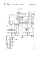
- FIG. 1A is a block diagram showing instruction fetch and dispatch in a known computing system
- FIG. 1B is a block diagram showing instruction fetch and dispatch in a known computing system
- FIG. 1C is a block diagram showing instruction fetch and dispatch in a known computing system
- FIG. 2A is a block diagram showing instruction fetch and dispatch in a particular embodiment of a computing system according to the present invention
- FIG. 2B is a block diagram showing instruction fetch and dispatch in a particular embodiment of a computing system according to the present invention.
- FIG. 2C is a block diagram showing instruction fetch and dispatch in a particular embodiment of a computing system according to the present invention.
- FIG. 2D is a block diagram showing instruction fetch and dispatch in a particular embodiment of a computing system according to the present invention.
- FIG. 3 is a block diagram of a particular embodiment of an apparatus according to the present invention for fetching and dispatching instructions
- FIG. 4 is a block diagram illustrating the operation of the instruction queuer of FIG. 3;
- FIG. 5 is a block diagram of an alternative embodiment of an apparatus according to the present invention for fetching and dispatching instructions
- FIG. 6 is a block diagram of a particular embodiment of an apparatus according to the present invention for predicting branches
- FIG. 7 is a block diagram of a particular embodiment of an entry in the branch cache shown in FIG. 5;
- FIG. 8A is a block diagram of a particular embodiment of the fetch stage of an instruction pipeline according to the present invention.
- FIG. 8B is a block diagram of a particular embodiment of the decode and address generation stages of an instruction pipeline according to the present invention.
- FIG. 8C is a block diagram of a particular embodiment of the executed and writeback stages of an instruction pipeline according to the present invention.
- FIGS. 2A-D are block diagrams showing instruction fetch and dispatch in a particular embodiment of a computing system according to the present invention.
- FIGS. 1A-D assume two instructions (A,B) are dispatched initially. However, unlike the example in FIGS. 1A-D, the two dispatched instructions (A,B) are immediately replaced by the next two sequential instructions (E,F) as shown in FIG. 2 B. Thus, four instructions are available for dispatch in the next clock cycle.
- a pointer 26 is used to keep track of which instruction follows the previously dispatched instructions in the program sequence. If three instructions are dispatched in the next clock cycle, as shown in FIG.
- line 14 C supplies instructions (G,H) and line 14 B supplies instruction (I) to dispatch register 18 in FIG. 2 C.
- the line which contains the next sequential program instruction to be loaded into dispatch register 18 may be termed the “leading quad”
- any next buffer line which simultaneously supplies instructions to dispatch register 18 to complete the fill operation may be termed the “trailing quad”.
- the leading quad is emptied by the fill operation, then the contents of the buffer may be advanced by one line as shown in FIG. 2 D.
- FIG. 2D two more instructions (F,G) are dispatched, and two instructions (J,K) are loaded in their place.
- FIG. 3 is a block diagram of a particular embodiment of an apparatus 30 for fetching and dispatching instructions according to the present invention.
- Apparatus 30 includes an instruction cache 34 which stores a plurality of lines of instructions that may be addressed by an address value received on a communication path 38 .
- each line stores four 32-bit instructions and communicates all the instructions in a line to a predecode circuit 42 over a communication path 46 .
- Predecode circuit partially decodes the four instructions and communicates the four partially decoded instructions to an instruction queuer 50 over a communication path 54 and to dispatch multiplexers 58 A-D over a queue bypass path 62 .
- Instruction queuer 50 includes four queue sections 66 A-D, one for each instruction in each line. All four queue sections have the same construction, so only the details of queue section 66 A shall be described.
- Queue section 66 A includes a plurality, e.g., six, serially connected.
- instruction buffers IBUF 0 -IBUF 5 Each instruction buffer is coupled to a multiplexer 68 through a corresponding multiplexer input path 70 A-F.
- Multiplexer 68 selects one of the instructions from among instruction buffers IBUF 0 -IBUF 5 in response to signals received over a line 72 A and communicates the selected instruction to a dispatch multiplexer 58 A over a communication path 74 A.
- the current instruction in register 22 A is also communicated to the input of dispatch multiplexer 58 A over a feedback communication path 76 A.
- Dispatch multiplexer 58 A thus selects from among the output of multiplexer 68 , queue bypass path 62 , or feedback communication path 76 A in response to signals received over a Q 0 MXSEL line 80 A to communicate an instruction to register 22 A over a communication path 82 A.
- Register 22 A then loads the received value in response to clock signals applied to the register (clocked registers are indicated by the angled symbol on the left side of each register), and then dispatches the instruction when possible.
- Queue sections 66 B-D also select instructions within one of their serially connected buffer sections in response to signals received over lines 72 B-D, respectively, and communicate the selected instructions to dispatch multiplexers 58 B-D over respective communication paths 74 B-D.
- Dispatch multiplexers 58 B-D communicate instructions, selected by signals received over Q 1 MXSEL-Q 3 MXSEL lines, to their respective registers 22 B-D over communication paths 82 B-D.
- Apparatus 30 selects which instructions are to be presented to dispatch register 18 in the following manner. The first time a line of instructions is retrieved from instruction cache 34 , instruction queuer 50 is empty, and multiplexers 58 A-D select the instructions from queue bypass path 62 . Instructions are then dispatched, and a new line of instructions are read from instruction cache 34 .
- a new line of instructions is read from instruction cache 34 on every clock cycle. If four instructions were dispatched every clock cycle, then dispatch. register would always be loaded from queue bypass path 62 . However, at any given cycle anywhere from zero to four instructions may be dispatched. Thus, if not all instructions are dispatched, then only certain ones of registers 22 A-D are loaded from queue bypass path 62 pursuant to the number of instructions dispatched.
- the previously read line of instructions is then loaded into IBUF 0 in each queue section 66 A-D, and a new line of instructions is read from instruction cache 34 . Thereafter, instructions are loaded from IBUF 0 in the appropriate queue section 66 A-D and from queue bypass path 62 .
- registers 22 A-B are loaded from queue bypass path 62 , registers 22 C-D are reloaded with the same instructions via communication paths 76 C-D, the previously read line of instructions is loaded into IBUF 0 in queue sections 66 A-D, and a new line of instructions is read from instruction cache 34 .
- register 22 C is loaded from IBUF 0 in queue section 66 C
- registers 22 A, 22 B, and 22 D are reloaded with the same instructions via communication paths 76 A, 76 C, and 76 D
- the line of instructions stored in IBUF 0 in each queue section 66 A-D is advanced to IBUF 1 in each queue section
- the previously read line of instructions is loaded into IBUF 0 in queue sections 66 A-D
- a new line is read from instruction cache 34 .
- the lines of instructions are advanced within queue sections 66 A-D until the buffer is full. At that time the apparatus stalls further loading of instruction lines into the queue. This manner of operation allows the instruction prefetch operation to be decoupled from the dispatch operation.
- a RDPTR register 86 stores a value I_STATE [ 4 : 0 ] for controlling the operation of instruction queuer 50 .
- STATE [ 4 : 2 ] is used to determine which buffer IBUF 0 -IBUF 5 in each queue section 66 A-D supplies the next instruction to registers 22 A-D, and STATE [ 1 : 0 ] functions as pointer 26 in FIGS. 2A-2C (a modulo- 4 counter) to indicate which instruction is to be dispatched next.
- An F_INST register 90 stores an INST_CONSUME value indicating how many instructions are consumed in every cycle (i.e., the sum of queuer register clock enables, or the total number of instructions dispatched from dispatch register 18 whether valid or not).
- the INST_CONSUME value is discussed in conjunction with FIG. 8 B.
- the INST_CONSUME value is added to STATE [ 4 : 0 ] by an adder 92 to point to the next instruction to be dispatched.
- STATE [ 4 : 2 ] is incremented every time the current line of instructions used to load dispatch register 18 is advanced in the queue.
- Queuer mux select circuit 98 presents the next four sequential instructions (in program order) to dispatch register 18 in accordance with the values of STATE [ 4 : 2 ] and STATE [ 1 : 0 ].
- FIG. 4 and Table 1 show which buffer in each queue section 66 A-D supplies the next instruction to its corresponding register 22 A-D in dispatch register 18 for the different values of STATE [ 1 : 0 ].
- registers 22 C and 22 D will be presented with the last two instructions in the leading quad (IBUF 3 ), and registers 22 A and 22 B will be presented with the first two instructions in the trailing quad (IBUF 2 ).
- the described apparatus for fetching and dispatching instructions may be used in many environments with or without modification. For example, assume integer, memory, and floating point instructions are stored in instruction cache 34 , and they may be mixed within a line of instructions. If there is a problem with resource contention and data dependencies with an instruction or type of instruction (e.g., floating point instructions), then those instructions may be dispatched into another queue where they can wait for the resource contention and data dependencies to clear without holding up dispatching of the other instructions.
- FIG. 5 is a block diagram of an alternative embodiment of an apparatus 104 according to the present invention for fetching and dispatching floating point instructions that may have been previously dispatched from dispatch register 18 in FIG. 3 . From inspection it is apparent that apparatus 104 operates much like apparatus 30 in FIG. 3, except apparatus 104 also provides for storing data together with the instructions to handle integer store operation data or floating point register data that is to be loaded from the integer register.
- FIG. 6 is a block diagram of a particular embodiment of an apparatus 110 according to the present invention for predicting branches.
- a branch prediction cache 114 is used to predict the outcome of branch instructions stored in instruction cache 34 .
- instruction cache 34 may be a 16 KB direct-mapped cache which outputs four instructions per cycle as noted above.
- branch prediction cache 114 is also direct mapped and may contain 1K entries (one entry per four instructions in instruction cache 34 ).
- Instruction cache 34 and branch cache 114 are accessed in parallel in the fetch stage of the pipeline through communication path 38 which receives an index (address) value from a counter 116 .
- instruction cache 34 and branch prediction cache 114 could be accessed with different addresses if desired.
- FIG. 7 shows a sample entry 120 from branch prediction cache 114 and an example of branch prediction.
- SRC source field
- DST destination field
- each branch instruction actually comprises two instructions.
- the first instruction termed the initial branch instruction, computes the branch target and the branch condition.
- the second instruction termed a delay instruction, immediately follows the initial branch instruction and is used to actually change the program flow to the branch target instruction.
- the source field 132 typically indicates the position of the delay instruction within the instruction line as shown in FIG. 7 .
- the value in source field 132 is communicated to a valid mask 158 through an OR circuit 150 . If the branch is predicted, valid mask 158 invalidates all instructions in the current line which occur after the delay instruction associated with the branch, since they would not be executed if the branch were taken. For example, if the delay instruction is the third instruction in the line as shown in FIG. 7, then the fourth instruction will be invalidated.
- the line (including any invalidated instructions) are communicated to instruction queuer 50 and queue bypass path 62 (FIG. 3 ), the value of the destination field is loaded into a register 152 , the value of counter 116 is loaded with the value from index field 128 , and instruction cache 34 is addressed to fetch the line which contains the predicted branch target instruction.
- the destination field in register 152 is then communicated to valid mask 158 through OR circuit 150 to invalidate the instructions which occur before the branch target instruction in the line. For example, if the branch target instruction is the second instruction in the line, then valid mask 158 invalidates the first instruction in the line.
- the line is then communicated to instruction queuer 50 and queue bypass path 62 .
- all branch prediction cache entries are initialized with a valid field of zero (branch not predicted).
- the result of each branch instruction is used to update the branch prediction cache entry (if necessary) by setting the valid bit to one, and by inserting the appropriate index, source, and destination values. Branch prediction thus may occur thereafter. If a branch previously taken is not taken at a later time, or if a branch not previously taken is taken at a later time, then the branch cache entry is updated (and correct instruction fetched) accordingly (discussed below).
- dispatch register 18 breaks (holds) the superscalar instructions which occur after the delay instruction of a predicted branch in dispatch register 18 to avoid mixing target instructions with a current branch instruction. Furthermore, dispatch register 18 breaks (holds) the superscalar instructions at the second branch when two branches are stored in dispatch register 18 so that only one branch at a time is allowed to execute.
- FIGS. 8A-8C are block diagrams of a particular embodiment of portions of an instruction pipeline according to the present invention showing how branch prediction operates. Where possible, reference numbers have been retained from previous figures.
- Instruction cache 34 may comprise an instruction memory and a tag memory as is well known in the art.
- the instruction memory portion may contain the lines of instructions, and the tag memory may contain the virtual address tags (and control information) associated with each line in the instruction memory. For the present discussion, only the tag memory portion ( 34 A) of instruction cache 34 is illustrated.
- Tag memory 34 A includes an application specific identification field (asid[ 7 : 0 ]), the instruction cache tag (tag[ 33 : 0 ], the high order 34 bits of the associated virtual address), a valid bit (V) and a region field (r[ 1 : 0 ]) for indicating the address space of the instruction.
- FIG. 8A shows the Fetch (F) stage of the instruction pipeline.
- Counters 116 A and 116 B are the primary F stage program counter which addresses tag memory 34 A and branch cache 114 .
- the value in counter 116 A (fpc[ 13 : 4 ]), which indexes a line in tag memory 34 A, is communicated to tag memory 34 A and to incrementing circuit 138 over communication path 38 A.
- Incrementing circuit 138 adds one to the counter value and communicates the incremented value to multiplexer 142 A and multiplexer 142 B over communication path 144 .
- Multiplexers 142 A and 142 B also receive the index field from branch cache 114 over communication path 148 , and a correction address (described below) over a communication path 160 .
- the value on communication path 160 (pc_jam-bus[ 13 : 2 ]) is used to correct branch misprediction, cache misses, etc.
- Multiplexer 142 B also receives a branch cache write address (bcwadr[ 13 : 4 ]) for updating the branch cache.
- the data used to update branch prediction cache 114 (bc_wdata[ 14 : 0 ]) is communicated to a register 164 over a communication path 168 .
- Multiplexers 142 A and 142 B select the appropriate address and communicate it to counters 116 A and 116 B, respectively.
- a register 172 stores a parallel load bit (f_pld) indicating whether counters 116 A-B were loaded with the incremented value from incrementing circuit 138 or whether counters 116 A-B were loaded from either communication path 148 or communication path 160
- a register 176 stores a value (fpc[ 3 : 2 ]) corresponding to the destination field of a branch prediction cache 114 entry (bits ( 4 : 3 ) of the bc( 14 : 3 ) data on communication path 148 ).
- registers 116 A, 172 , and 176 are combined with the output of tag memory 34 A and stored in a queue register TBUF 0 , which is one of six registers (TBUF 0 -TBUF 5 ) used to store tag data to correspond to the six instruction buffers IBUF 0 -IBUF 5 in instruction queuer 50 .
- Each register TBUF 0 -TBUF 5 is coupled to multiplexers 180 and 184 which select the registers which correspond to the leading quad and trailing quad, respectively, in instruction queuer 50 .
- the leading quad tag memory information is communicated to the next stage in the pipeline over a communication path 188
- the trailing quad tag memory information is communicated to the next stage in the pipeline over a communication path 190 .
- FIG. 8B shows the Decode (D) and Address Generation (A) stages of the instruction pipeline.
- bits [ 56 : 2 ] of the leading quad information from tag memory 34 A is stored in a DLTAG register 200
- the trailing quad information from tag memory 34 A is stored in a DTTAG register 204 .
- the destination field of the branch prediction cache 114 entry (fpc[ 3 : 2 ]), if any, associated with the leading quad information is communicated to a multiplexer 208 .
- the other input to multiplexer 208 is coupled to an output communication path 210 of an adder 214 which contains the pointer value of the position of the next sequential instruction to be dispatched during normal sequential execution.
- Multiplexer 208 selects either the destination value or the next sequential instruction value and communicates the selected value to the output communication path 216 of DLTAG register 200 .
- Communication path 216 is coupled to an input of a multiplexer 218 .
- the trailing quad tag memory information stored in DTTAG register 204 is communicated to multiplexer 218 and to a compare circuit 220 over a communication path 224 .
- Multiplexer 218 selects the tag information corresponding to the first instruction to be executed next and outputs the selected information on a communication path 226 to an ATAG register 227 in the A stage of the pipeline.
- the dispatch register pointer value is communicated to adder 214 over a communication path 228 , the tag memory information is communicated to compare circuit 220 over a communication path 230 , and the instruction cache index is communicated to a compare circuit 234 .
- Compare circuit 220 compares the leading quad tag to the trailing quad tag. If they do not match, then the leading quad instructions and the trailing quad instructions come from a different context, so they should not be dispatched simultaneously. A signal is provided on a communication path 238 to break the superscalar instructions when this occurs.
- Compare circuit 234 compares the instruction cache index to the hex value “FFF” to determine if the end of the instruction cache is being addressed. If so, then it is desirable to break the superscalar instructions at the end of the cache line, and a signal is provided on a communication path 242 for that purpose.
- Adder 214 receives a value indicating the sum of valid instructions dispatched over a communication path 250 , and that value is used to increment the current dispatch register pointer value to produce the updated dispatch register pointer value on communication path 210 .
- register 90 (see also FIG. 3) is loaded with the value indicating the number of instructions consumed (both valid and invalid instructions), and this value is used to control the operation of instruction queuer 50 as discussed in conjunction with FIG. 3 .
- the actual branch address is generated. Since each branch instruction comprises an initial branch instruction followed by a delay instruction, and since the actual branch is accomplished after the delay instruction, the branch target address must be calculated relative to the delay instruction. Accordingly, when the tag information corresponding to the line containing the branch instruction is stored in ATAG register 227 , a value indicating the relative position of the delay instruction within the line is selected by a multiplexer 249 and stored in a RELDLY register 254 via a communication path 258 . The relative delay value is communicated to a branch target adder 260 over a communication path 264 .
- Branch target adder 260 also receives the ATAG register 227 value (which is the address of the first instruction in the line) via a communication path 268 , and an offset value from an AOFFSET register 272 via a communication path 276 .
- AOFFSET register 272 receives the 26-bit offset value from the branch instruction over a communication path 280 , and subjects bits [ 17 : 2 ] of the offset value to a sign extension function in a sign extension circuit 284 (if necessary) prior to forwarding the offset value to branch target adder 260 .
- AOFFSET register 272 also communicates the 26-bit offset value to a multiplexer 288 which also receives bits [ 27 : 2 ] of the branch target address calculated by branch target adder 260 over a communication path 292 . Multiplexer 288 thus allows bits [ 27 : 2 ] of the calculated branch target address to be replaced by the offset value stored in AOFFSET register 272 .
- branch target adder 260 The output from branch target adder 260 is communicated to one input of a multiplexer 289 .
- the other input to multiplexer 289 is a branch target address from a JUMP or JUMP REGISTER instruction received over a communication path 296 coupled to the general purpose register file.
- the selected branch target address will be the output from branch target adder 260 (possibly modified by multiplexer 288 ) unless the branch was caused by a JUMP or JUMP REGISTER instruction, in which case the address specified by the appropriate register will take precedence.
- the reason for the specific structure of the branch target address calculating circuits arises from the way the branch target addresses are calculated from the different types of branch instructions, namely a regular branch, JUMP, and JUMP REGISTER.
- a regular branch instruction the relative delay register value, the ATAG register value, and the offset value are added together to create the branch target address;
- the ATAG and REL_DLY register values are added, and the offset value is concatenated to the sum; and for a JUMP REGISTER instruction, the register value from communication path 296 is used for the branch target address.
- the values from ATAG register 227 and RELDLY register 254 are also communicated to a return address adder 300 .
- Return address adder 300 is used to calculate the return address when a branch results in the execution of a subroutine. After the subroutine is finished, it is desirable to return to the instruction immediately following the instruction which called it. Thus, return address adder 300 adds +1 to the addition of the tag, index, and relative delay to produce the address of the instruction following the delay slot of the branch instruction which called the subroutine.
- the return address is output on a communication path 304 .
- FIG. 8C shows the Execute (E) and Writeback (W) stages of the pipeline.
- the contents of ATAG register 227 are communicated to an ETAG register 318 over a communication path 308 and to a compare circuit 341 over a communication path 309
- the contents of RELDLY register 254 are communicated to an E_REL_DLY register 322 over a communication path 312
- the calculated return address from return address adder 300 is communicated to a link value (LNVAL) register 326 over communication path 304
- the selected branch target address from multiplexer 289 is communicated to a BR_TARG register 330 over communication path 314 .
- LNVAL link value
- An EPC register 334 stores the real address of the instruction the program is supposed to execute in the E stage, and an ASID register stores the program-controlled ASID of the instruction to be executed together with a coherence value (c[ 2 : 0 ]) which typically indicates whether the data used by the instruction is cacheable or not.
- the ASID and tag stored in ETAG register 318 are compared to the ASID and tag from ASID register 338 and EPC register 334 (corresponding to the instruction that is actually supposed to be executed) by a compare circuit 339 to determine if the actual instruction expected to be executed (where the program should be) is actually the instruction fetched from the instruction cache. If the values do not match, then an instruction cache miss signal is provided on a communication path 340 .
- the value in ATAG register 227 corresponds to the line containing the predicted branch target instruction
- the value in BR_TARG register 330 corresponds to the actual branch target address.
- the index and destination field (the predicted branch target address) received from ATAG register 227 over communication path 309 is compared to the calculated branch target address received from BT_TARG register 330 over a communication path 343 by a compare circuit 341 to determine whether the actual branch target instruction expected to be executed corresponds to the predicted branch target instruction fetched from the instruction cache. If the values do not match, then a branch cache miss (branch misprediction) signal is provided on a communication path 345 .
- EPC register 334 The value in EPC register 334 is communicated to a WPC register 354 in the writeback stage of the pipeline and to one input of a multiplexer 362 over a communication path 358 .
- the other input to multiplexer 362 receives the value in WPC register 354 (the original value of EPC register 334 delayed by one cycle) over a communication path 366 .
- Multiplexer 362 selects one of theses values and communicates the selected value to one input of an EPC adder 350 .
- EPC adder 350 is responsible for updating the value from EPC register 334 during normal operation.
- the value of EPC register 334 ordinarily is selected during normal operation, and the value of WPC register 354 is selected for exception processing.
- the other input to EPC adder 350 is coupled to a multiplexer 366 .
- One input to multiplexer 366 is the number of valid instructions dispatched from dispatch register 18
- the other input is an exception adjustment value from multiplexer 369 ( ⁇ 1 to +3).
- the value from EPC register 334 is incremented by the number of valid instructions dispatched from dispatch register 18 so that the value in EPC register 334 points to the next instruction to be executed.
- an exception occurs (trap, instruction cache miss, etc)
- the exception adjustment value is added to the value in WPC register 354 to indicate the instruction which caused the exception.
- the value ⁇ 1 is used when the exception was caused by a delay instruction, since in that case it is desirable to point to the branch instruction immediately before it.
- EPC-COP register 370 The value indicating which instruction caused the exception is stored in an EPC-COP register 370 , which is reloaded with it's present value until another exception occurs via multiplexer 374 .
- a TRAP-BASE register 376 stores an address that the program should go to when an exception occurs and communicates the value to a multiplexer 377 .
- the other input to multiplexer 377 is a reset vector value. One of these values is selected and output on a communication path 379 .
- a multiplexer 380 receives the value from EPC-COP register 370 over a communication path 384 when returning from an exception, a vector address from communication path 379 on an exception condition, the calculated branch target address over a communication path 388 for branches, the EPC value from communication path 358 to hold the EPC value during an instruction cache miss, and the updated EPC value over communication path 396 .
- the selected value is output on a communication path 430 (PC_JAM_BUS[ 47 : 0 ]), of which bits [ 13 : 2 ] are the correction values supplied to the F stage circuitry shown in FIG. 8A to correctly index the instruction cache, tag memory 34 A and branch prediction cache 114 .
- the updated EPC value is selected by multiplexer 380 and loaded into EPC register 334 .
- multiplexer 380 selects the calculated branch target address and communicates the new branch target address to branch cache 114 via communication path 160 (FIG. 8 A).
- the write address used to update branch prediction cache 114 is calculated by a branch cache address adder 400 which adds the value in EPC register 334 to the value in E_REL_DLY register 322 and produces the write address on a communication path 404 .
- the value of bits [ 3 : 2 ] on communication path 404 correspond to the position of the delay instruction and may be used as the source field in the branch prediction cache entry.
- the remaining write data on communication path 168 comprises bits [ 13 : 2 ] of the calculated branch target address, which is the updated index and destination field entries.
Abstract
Description
| TABLE 1 | |||||
| STATE | |||||
| [1:0] | Q0MXSEL | | Q2MXSEL | Q3MXSEL | |
| 0 | STATE | STATE | STATE | STATE[4:2] | |
| [4:2] | [4:2] | [4:2] | |||
| 1 | STATE | STATE | STATE | STATE[4:2] | |
| [4:2]-1 | [4:2] | [4:2] | |||
| 2 | STATE | STATE | STATE | STATE[4:2] | |
| [4:2]-1 | [4:2]-1 | [4:2] | |||
| 3 | STATE | STATE | STATE | STATE[4:2] | |
| [4:2]-1 | [4:2]-1 | [4:2]-1 | |||
Claims (23)
Priority Applications (2)
| Application Number | Priority Date | Filing Date | Title |
|---|---|---|---|
| US09/363,635 US6247124B1 (en) | 1993-12-15 | 1999-07-30 | Branch prediction entry with target line index calculated using relative position of second operation of two step branch operation in a line of instructions |
| US09/863,898 US6691221B2 (en) | 1993-12-15 | 2001-05-24 | Loading previously dispatched slots in multiple instruction dispatch buffer before dispatching remaining slots for parallel execution |
Applications Claiming Priority (4)
| Application Number | Priority Date | Filing Date | Title |
|---|---|---|---|
| US08/168,744 US5604909A (en) | 1993-12-15 | 1993-12-15 | Apparatus for processing instructions in a computing system |
| US47694295A | 1995-06-07 | 1995-06-07 | |
| US08/781,851 US5954815A (en) | 1993-12-15 | 1997-01-10 | Invalidating instructions in fetched instruction blocks upon predicted two-step branch operations with second operation relative target address |
| US09/363,635 US6247124B1 (en) | 1993-12-15 | 1999-07-30 | Branch prediction entry with target line index calculated using relative position of second operation of two step branch operation in a line of instructions |
Related Parent Applications (1)
| Application Number | Title | Priority Date | Filing Date |
|---|---|---|---|
| US08/781,851 Continuation US5954815A (en) | 1993-12-15 | 1997-01-10 | Invalidating instructions in fetched instruction blocks upon predicted two-step branch operations with second operation relative target address |
Related Child Applications (1)
| Application Number | Title | Priority Date | Filing Date |
|---|---|---|---|
| US09/863,898 Continuation US6691221B2 (en) | 1993-12-15 | 2001-05-24 | Loading previously dispatched slots in multiple instruction dispatch buffer before dispatching remaining slots for parallel execution |
Publications (1)
| Publication Number | Publication Date |
|---|---|
| US6247124B1 true US6247124B1 (en) | 2001-06-12 |
Family
ID=22612755
Family Applications (4)
| Application Number | Title | Priority Date | Filing Date |
|---|---|---|---|
| US08/168,744 Expired - Lifetime US5604909A (en) | 1993-12-15 | 1993-12-15 | Apparatus for processing instructions in a computing system |
| US08/781,851 Expired - Lifetime US5954815A (en) | 1993-12-15 | 1997-01-10 | Invalidating instructions in fetched instruction blocks upon predicted two-step branch operations with second operation relative target address |
| US09/363,635 Expired - Lifetime US6247124B1 (en) | 1993-12-15 | 1999-07-30 | Branch prediction entry with target line index calculated using relative position of second operation of two step branch operation in a line of instructions |
| US09/863,898 Expired - Fee Related US6691221B2 (en) | 1993-12-15 | 2001-05-24 | Loading previously dispatched slots in multiple instruction dispatch buffer before dispatching remaining slots for parallel execution |
Family Applications Before (2)
| Application Number | Title | Priority Date | Filing Date |
|---|---|---|---|
| US08/168,744 Expired - Lifetime US5604909A (en) | 1993-12-15 | 1993-12-15 | Apparatus for processing instructions in a computing system |
| US08/781,851 Expired - Lifetime US5954815A (en) | 1993-12-15 | 1997-01-10 | Invalidating instructions in fetched instruction blocks upon predicted two-step branch operations with second operation relative target address |
Family Applications After (1)
| Application Number | Title | Priority Date | Filing Date |
|---|---|---|---|
| US09/863,898 Expired - Fee Related US6691221B2 (en) | 1993-12-15 | 2001-05-24 | Loading previously dispatched slots in multiple instruction dispatch buffer before dispatching remaining slots for parallel execution |
Country Status (8)
| Country | Link |
|---|---|
| US (4) | US5604909A (en) |
| EP (2) | EP1320031A3 (en) |
| JP (1) | JP2815237B2 (en) |
| KR (1) | KR100212204B1 (en) |
| CN (2) | CN1267819C (en) |
| DE (1) | DE69433621T2 (en) |
| HK (1) | HK1013153A1 (en) |
| WO (1) | WO1995016954A1 (en) |
Cited By (21)
| Publication number | Priority date | Publication date | Assignee | Title |
|---|---|---|---|---|
| US20040003216A1 (en) * | 2002-06-28 | 2004-01-01 | Fujitsu Limited | Branch prediction apparatus and method |
| US20050102483A1 (en) * | 2002-10-22 | 2005-05-12 | Kinter Ryan C. | Apparatus and method for discovering a scratch pad memory configuration |
| US20050216703A1 (en) * | 2004-03-26 | 2005-09-29 | International Business Machines Corporation | Apparatus and method for decreasing the latency between an instruction cache and a pipeline processor |
| US20060106987A1 (en) * | 2004-11-18 | 2006-05-18 | International Business Machines Corporation | Load address dependency mechanism system and method in a high frequency, low power processor system |
| US20070101111A1 (en) * | 2005-10-31 | 2007-05-03 | Mips Technologies, Inc. | Processor core and method for managing program counter redirection in an out-of-order processor pipeline |
| US20070101110A1 (en) * | 2005-10-31 | 2007-05-03 | Mips Technologies, Inc. | Processor core and method for managing branch misprediction in an out-of-order processor pipeline |
| US20070204135A1 (en) * | 2006-02-28 | 2007-08-30 | Mips Technologies, Inc. | Distributive scoreboard scheduling in an out-of order processor |
| US20070234089A1 (en) * | 2002-08-16 | 2007-10-04 | Schmit Herman H | Programmable pipeline fabric having mechanism to terminate signal propagation |
| US20080016326A1 (en) * | 2006-07-14 | 2008-01-17 | Mips Technologies, Inc. | Latest producer tracking in an out-of-order processor, and applications thereof |
| US20080046653A1 (en) * | 2006-08-18 | 2008-02-21 | Mips Technologies, Inc. | Methods for reducing data cache access power in a processor, and applications thereof |
| US20080059771A1 (en) * | 2006-09-06 | 2008-03-06 | Mips Technologies, Inc. | Out-of-order processor having an in-order coprocessor, and applications thereof |
| US20080059765A1 (en) * | 2006-09-06 | 2008-03-06 | Mips Technologies, Inc. | Coprocessor interface unit for a processor, and applications thereof |
| US20080082793A1 (en) * | 2006-09-29 | 2008-04-03 | Mips Technologies, Inc. | Detection and prevention of write-after-write hazards, and applications thereof |
| US20080082794A1 (en) * | 2006-09-29 | 2008-04-03 | Mips Technologies, Inc. | Load/store unit for a processor, and applications thereof |
| US20080082721A1 (en) * | 2006-09-29 | 2008-04-03 | Mips Technologies, Inc. | Data cache virtual hint way prediction, and applications thereof |
| US7370178B1 (en) | 2006-07-14 | 2008-05-06 | Mips Technologies, Inc. | Method for latest producer tracking in an out-of-order processor, and applications thereof |
| US7539879B2 (en) * | 2002-12-04 | 2009-05-26 | Nxp B.V. | Register file gating to reduce microprocessor power dissipation |
| US7650465B2 (en) | 2006-08-18 | 2010-01-19 | Mips Technologies, Inc. | Micro tag array having way selection bits for reducing data cache access power |
| US20110213951A1 (en) * | 2005-02-02 | 2011-09-01 | International Business Machines Corporation | Storing Branch Information in an Address Table of a Processor |
| US8078846B2 (en) | 2006-09-29 | 2011-12-13 | Mips Technologies, Inc. | Conditional move instruction formed into one decoded instruction to be graduated and another decoded instruction to be invalidated |
| US9851975B2 (en) | 2006-02-28 | 2017-12-26 | Arm Finance Overseas Limited | Compact linked-list-based multi-threaded instruction graduation buffer |
Families Citing this family (55)
| Publication number | Priority date | Publication date | Assignee | Title |
|---|---|---|---|---|
| US5734874A (en) * | 1994-04-29 | 1998-03-31 | Sun Microsystems, Inc. | Central processing unit with integrated graphics functions |
| US5778250A (en) * | 1994-05-23 | 1998-07-07 | Cirrus Logic, Inc. | Method and apparatus for dynamically adjusting the number of stages of a multiple stage pipeline |
| WO1996012231A1 (en) | 1994-10-14 | 1996-04-25 | Silicon Graphics, Inc. | A translation buffer for detecting and preventing conflicting virtual addresses from being stored therein |
| EP0803095A1 (en) | 1994-10-14 | 1997-10-29 | Silicon Graphics, Inc. | Indexing and multiplexing of interleaved cache memory arrays |
| US5991869A (en) * | 1995-04-12 | 1999-11-23 | Advanced Micro Devices, Inc. | Superscalar microprocessor including a high speed instruction alignment unit |
| GB9521977D0 (en) * | 1995-10-26 | 1996-01-03 | Sgs Thomson Microelectronics | Cache memory |
| GB9521980D0 (en) * | 1995-10-26 | 1996-01-03 | Sgs Thomson Microelectronics | Branch target buffer |
| GB9521955D0 (en) * | 1995-10-26 | 1996-01-03 | Sgs Thomson Microelectronics | Cache memory |
| US6216213B1 (en) * | 1996-06-07 | 2001-04-10 | Motorola, Inc. | Method and apparatus for compression, decompression, and execution of program code |
| WO1998002798A1 (en) * | 1996-07-16 | 1998-01-22 | Advanced Micro Devices, Inc. | A superscalar microprocesser including a high speed instruction alignment unit |
| DE19630861A1 (en) * | 1996-07-31 | 1998-02-05 | Philips Patentverwaltung | Data processing device with a microprocessor and an additional computing unit |
| US5859992A (en) * | 1997-03-12 | 1999-01-12 | Advanced Micro Devices, Inc. | Instruction alignment using a dispatch list and a latch list |
| US6157999A (en) * | 1997-06-03 | 2000-12-05 | Motorola Inc. | Data processing system having a synchronizing link stack and method thereof |
| US5964869A (en) * | 1997-06-19 | 1999-10-12 | Sun Microsystems, Inc. | Instruction fetch mechanism with simultaneous prediction of control-flow instructions |
| US5935238A (en) * | 1997-06-19 | 1999-08-10 | Sun Microsystems, Inc. | Selection from multiple fetch addresses generated concurrently including predicted and actual target by control-flow instructions in current and previous instruction bundles |
| US6157988A (en) * | 1997-08-01 | 2000-12-05 | Micron Technology, Inc. | Method and apparatus for high performance branching in pipelined microsystems |
| US6185676B1 (en) * | 1997-09-30 | 2001-02-06 | Intel Corporation | Method and apparatus for performing early branch prediction in a microprocessor |
| US6243805B1 (en) * | 1998-08-11 | 2001-06-05 | Advanced Micro Devices, Inc. | Programming paradigm and microprocessor architecture for exact branch targeting |
| US6289442B1 (en) * | 1998-10-05 | 2001-09-11 | Advanced Micro Devices, Inc. | Circuit and method for tagging and invalidating speculatively executed instructions |
| US6442674B1 (en) * | 1998-12-30 | 2002-08-27 | Intel Corporation | Method and system for bypassing a fill buffer located along a first instruction path |
| US6957327B1 (en) * | 1998-12-31 | 2005-10-18 | Stmicroelectronics, Inc. | Block-based branch target buffer |
| US6185672B1 (en) * | 1999-02-19 | 2001-02-06 | Advanced Micro Devices, Inc. | Method and apparatus for instruction queue compression |
| EP1050810A1 (en) | 1999-05-03 | 2000-11-08 | STMicroelectronics SA | A computer system comprising multiple functional units |
| KR20020039689A (en) * | 1999-10-14 | 2002-05-27 | 토토라노 제이. 빈센트 | Apparatus and method for caching alignment information |
| US6636959B1 (en) | 1999-10-14 | 2003-10-21 | Advanced Micro Devices, Inc. | Predictor miss decoder updating line predictor storing instruction fetch address and alignment information upon instruction decode termination condition |
| US6546478B1 (en) | 1999-10-14 | 2003-04-08 | Advanced Micro Devices, Inc. | Line predictor entry with location pointers and control information for corresponding instructions in a cache line |
| US6647490B2 (en) | 1999-10-14 | 2003-11-11 | Advanced Micro Devices, Inc. | Training line predictor for branch targets |
| US6591361B1 (en) | 1999-12-28 | 2003-07-08 | International Business Machines Corporation | Method and apparatus for converting data into different ordinal types |
| US7149883B1 (en) | 2000-03-30 | 2006-12-12 | Intel Corporation | Method and apparatus selectively to advance a write pointer for a queue based on the indicated validity or invalidity of an instruction stored within the queue |
| US6857061B1 (en) | 2000-04-07 | 2005-02-15 | Nintendo Co., Ltd. | Method and apparatus for obtaining a scalar value directly from a vector register |
| US6701424B1 (en) * | 2000-04-07 | 2004-03-02 | Nintendo Co., Ltd. | Method and apparatus for efficient loading and storing of vectors |
| US6859862B1 (en) | 2000-04-07 | 2005-02-22 | Nintendo Co., Ltd. | Method and apparatus for software management of on-chip cache |
| US6484228B2 (en) | 2000-04-19 | 2002-11-19 | Motorola, Inc. | Method and apparatus for data compression and decompression for a data processor system |
| DE10043003A1 (en) * | 2000-09-01 | 2002-03-14 | Infineon Technologies Ag | Program controlled unit |
| US7035998B1 (en) | 2000-11-03 | 2006-04-25 | Mips Technologies, Inc. | Clustering stream and/or instruction queues for multi-streaming processors |
| US7139898B1 (en) * | 2000-11-03 | 2006-11-21 | Mips Technologies, Inc. | Fetch and dispatch disassociation apparatus for multistreaming processors |
| JP2002318687A (en) * | 2001-04-18 | 2002-10-31 | Fujitsu Ltd | Information processor and computer system |
| US20040111594A1 (en) * | 2002-12-05 | 2004-06-10 | International Business Machines Corporation | Multithreading recycle and dispatch mechanism |
| JP3855270B2 (en) * | 2003-05-29 | 2006-12-06 | ソニー株式会社 | Antenna mounting method |
| DE102005009083B4 (en) * | 2005-02-28 | 2007-05-10 | Infineon Technologies Ag | Multithread processor with a synchronization unit and method of operating such |
| US20060229638A1 (en) * | 2005-03-29 | 2006-10-12 | Abrams Robert M | Articulating retrieval device |
| US7461237B2 (en) * | 2005-04-20 | 2008-12-02 | Sun Microsystems, Inc. | Method and apparatus for suppressing duplicative prefetches for branch target cache lines |
| US20070198812A1 (en) * | 2005-09-27 | 2007-08-23 | Ibm Corporation | Method and apparatus for issuing instructions from an issue queue including a main issue queue array and an auxiliary issue queue array in an information handling system |
| US7350056B2 (en) * | 2005-09-27 | 2008-03-25 | International Business Machines Corporation | Method and apparatus for issuing instructions from an issue queue in an information handling system |
| US7711935B2 (en) | 2007-04-30 | 2010-05-04 | Netlogic Microsystems, Inc. | Universal branch identifier for invalidation of speculative instructions |
| US8127115B2 (en) * | 2009-04-03 | 2012-02-28 | International Business Machines Corporation | Group formation with multiple taken branches per group |
| US9354887B2 (en) * | 2010-06-28 | 2016-05-31 | International Business Machines Corporation | Instruction buffer bypass of target instruction in response to partial flush |
| US8937622B2 (en) | 2010-09-20 | 2015-01-20 | Qualcomm Incorporated | Inter-processor communication techniques in a multiple-processor computing platform |
| US9280398B2 (en) | 2012-01-31 | 2016-03-08 | International Business Machines Corporation | Major branch instructions |
| US9229722B2 (en) | 2012-01-31 | 2016-01-05 | International Business Machines Corporation | Major branch instructions with transactional memory |
| US9304932B2 (en) | 2012-12-20 | 2016-04-05 | Qualcomm Incorporated | Instruction cache having a multi-bit way prediction mask |
| WO2015061648A1 (en) * | 2013-10-25 | 2015-04-30 | Advanced Micro Devices, Inc. | Bandwidth increase in branch prediction unit and level 1 instruction cache |
| US10216520B2 (en) * | 2014-10-06 | 2019-02-26 | Via Technologies, Inc. | Compressing instruction queue for a microprocessor |
| JP7004905B2 (en) * | 2018-03-26 | 2022-01-21 | 富士通株式会社 | Arithmetic processing unit and control method of arithmetic processing unit |
| CN109101276B (en) | 2018-08-14 | 2020-05-05 | 阿里巴巴集团控股有限公司 | Method for executing instruction in CPU |
Citations (36)
| Publication number | Priority date | Publication date | Assignee | Title |
|---|---|---|---|---|
| JPS50152629A (en) | 1974-05-27 | 1975-12-08 | ||
| JPS5729153A (en) | 1980-07-29 | 1982-02-17 | Fujitsu Ltd | Control system for instruction processing order |
| JPS57152046A (en) | 1981-03-13 | 1982-09-20 | Mitsubishi Electric Corp | Instruction buffer controlling method |
| JPS5991549A (en) | 1982-11-17 | 1984-05-26 | Nec Corp | Method for storing instruction word to instruction buffer |
| EP0116883A2 (en) | 1983-02-18 | 1984-08-29 | Siemens Nixdorf Informationssysteme Aktiengesellschaft | Circuit arrangement for buffering command words |
| US4580214A (en) | 1982-03-02 | 1986-04-01 | Hitachi, Ltd. | Memory control system |
| US4635194A (en) | 1983-05-02 | 1987-01-06 | International Business Machines Corporation | Instruction buffer bypass apparatus |
| US4682284A (en) | 1984-12-06 | 1987-07-21 | American Telephone & Telegraph Co., At&T Bell Lab. | Queue administration method and apparatus |
| EP0240870A2 (en) | 1986-04-11 | 1987-10-14 | Symbolics, Inc. | Instruction prefetch unit |
| US4777587A (en) | 1985-08-30 | 1988-10-11 | Advanced Micro Devices, Inc. | System for processing single-cycle branch instruction in a pipeline having relative, absolute, indirect and trap addresses |
| EP0372865A2 (en) | 1988-12-05 | 1990-06-13 | Matsushita Electric Industrial Co., Ltd. | Cache device for supplying a fixed word length of a variable length instruction code and instruction fetch device |
| EP0380854A2 (en) | 1989-02-03 | 1990-08-08 | Digital Equipment Corporation | Instruction buffer system for a digital computer |
| US4984154A (en) | 1982-11-17 | 1991-01-08 | Nec Corporation | Instruction prefetching device with prediction of a branch destination address |
| US5043868A (en) | 1984-02-24 | 1991-08-27 | Fujitsu Limited | System for by-pass control in pipeline operation of computer |
| EP0477598A2 (en) | 1990-09-26 | 1992-04-01 | Siemens Aktiengesellschaft | Instruction unit for a processor featuring 'n' processing elements |
| US5121502A (en) * | 1989-12-20 | 1992-06-09 | Hewlett-Packard Company | System for selectively communicating instructions from memory locations simultaneously or from the same memory locations sequentially to plurality of processing |
| US5133077A (en) | 1987-10-19 | 1992-07-21 | International Business Machines Corporation | Data processor having multiple execution units for processing plural classs of instructions in parallel |
| US5136697A (en) | 1989-06-06 | 1992-08-04 | Advanced Micro Devices, Inc. | System for reducing delay for execution subsequent to correctly predicted branch instruction using fetch information stored with each block of instructions in cache |
| JPH04247522A (en) | 1991-02-04 | 1992-09-03 | Toshiba Corp | Parallel operation processor |
| DE4211222A1 (en) | 1991-04-05 | 1992-10-22 | Toshiba Kawasaki Kk | Branch instruction target controller for super-scaling processor system - has branch target buffer providing tabulated group of instructions with instruction checking unit |
| JPH04328636A (en) | 1991-04-30 | 1992-11-17 | Toshiba Corp | Instruction distribution processor for parallel processor |
| DE4216905A1 (en) | 1991-06-24 | 1993-01-07 | Mitsubishi Electric Corp | Super-scaler processor for parallel high speed operations - has selector with control on basis of empty registers to provide improved parallel processor without unwanted delays |
| US5233694A (en) | 1988-11-11 | 1993-08-03 | Hitachi, Ltd. | Pipelined data processor capable of performing instruction fetch stages of a plurality of instructions simultaneously |
| US5247628A (en) | 1987-11-30 | 1993-09-21 | International Business Machines Corporation | Parallel processor instruction dispatch apparatus with interrupt handler |
| US5267350A (en) | 1989-10-26 | 1993-11-30 | Kenji Matsubara | Method for fetching plural instructions using single fetch request in accordance with empty state of instruction buffers and setting of flag latches |
| US5283873A (en) | 1990-06-29 | 1994-02-01 | Digital Equipment Corporation | Next line prediction apparatus for a pipelined computed system |
| US5297281A (en) | 1989-04-24 | 1994-03-22 | International Business Machines Corporation | Multiple sequence processor system |
| US5299321A (en) | 1990-12-18 | 1994-03-29 | Oki Electric Industry Co., Ltd. | Parallel processing device to operate with parallel execute instructions |
| US5317701A (en) | 1990-01-02 | 1994-05-31 | Motorola, Inc. | Method for refilling instruction queue by reading predetermined number of instruction words comprising one or more instructions and determining the actual number of instruction words used |
| US5333281A (en) | 1988-03-04 | 1994-07-26 | Nec Corporation | Advanced instruction execution system for assigning different indexes to instructions capable of parallel execution and same indexes to instructions incapable of parallel execution |
| US5367703A (en) | 1993-01-08 | 1994-11-22 | International Business Machines Corporation | Method and system for enhanced branch history prediction accuracy in a superscalar processor system |
| US5390355A (en) * | 1989-05-24 | 1995-02-14 | Tandem Computers Incorporated | Computer architecture capable of concurrent issuance and execution of general purpose multiple instructions |
| US5404552A (en) | 1991-03-01 | 1995-04-04 | Mitsubishi Denki Kabushiki Kaisha | Pipeline risc processing unit with improved efficiency when handling data dependency |
| US5553254A (en) | 1993-01-15 | 1996-09-03 | International Business Machines Corporation | Instruction cache access and prefetch process controlled by a predicted instruction-path mechanism |
| US5835746A (en) * | 1997-04-21 | 1998-11-10 | Motorola, Inc. | Method and apparatus for fetching and issuing dual-word or multiple instructions in a data processing system |
| US5978896A (en) * | 1993-01-08 | 1999-11-02 | International Business Machines Corporation | Method and system for increased instruction dispatch efficiency in a superscalar processor system |
Family Cites Families (3)
| Publication number | Priority date | Publication date | Assignee | Title |
|---|---|---|---|---|
| US5185868A (en) * | 1990-01-16 | 1993-02-09 | Advanced Micro Devices, Inc. | Apparatus having hierarchically arranged decoders concurrently decoding instructions and shifting instructions not ready for execution to vacant decoders higher in the hierarchy |
| US5680564A (en) * | 1995-05-26 | 1997-10-21 | National Semiconductor Corporation | Pipelined processor with two tier prefetch buffer structure and method with bypass |
| US6065110A (en) * | 1998-02-09 | 2000-05-16 | International Business Machines Corporation | Method and apparatus for loading an instruction buffer of a processor capable of out-of-order instruction issue |
-
1993
- 1993-12-15 US US08/168,744 patent/US5604909A/en not_active Expired - Lifetime
-
1994
- 1994-12-15 DE DE69433621T patent/DE69433621T2/en not_active Expired - Lifetime
- 1994-12-15 CN CNB021407622A patent/CN1267819C/en not_active Expired - Lifetime
- 1994-12-15 EP EP03003266A patent/EP1320031A3/en not_active Withdrawn
- 1994-12-15 KR KR1019950703432A patent/KR100212204B1/en not_active IP Right Cessation
- 1994-12-15 EP EP95902965A patent/EP0690373B1/en not_active Expired - Lifetime
- 1994-12-15 WO PCT/JP1994/002112 patent/WO1995016954A1/en active IP Right Grant
- 1994-12-15 JP JP7516669A patent/JP2815237B2/en not_active Expired - Lifetime
- 1994-12-15 CN CN94191180A patent/CN1104680C/en not_active Expired - Lifetime
-
1997
- 1997-01-10 US US08/781,851 patent/US5954815A/en not_active Expired - Lifetime
-
1998
- 1998-12-21 HK HK98114187A patent/HK1013153A1/en not_active IP Right Cessation
-
1999
- 1999-07-30 US US09/363,635 patent/US6247124B1/en not_active Expired - Lifetime
-
2001
- 2001-05-24 US US09/863,898 patent/US6691221B2/en not_active Expired - Fee Related
Patent Citations (38)
| Publication number | Priority date | Publication date | Assignee | Title |
|---|---|---|---|---|
| JPS50152629A (en) | 1974-05-27 | 1975-12-08 | ||
| JPS5729153A (en) | 1980-07-29 | 1982-02-17 | Fujitsu Ltd | Control system for instruction processing order |
| JPS57152046A (en) | 1981-03-13 | 1982-09-20 | Mitsubishi Electric Corp | Instruction buffer controlling method |
| US4580214A (en) | 1982-03-02 | 1986-04-01 | Hitachi, Ltd. | Memory control system |
| US4984154A (en) | 1982-11-17 | 1991-01-08 | Nec Corporation | Instruction prefetching device with prediction of a branch destination address |
| JPS5991549A (en) | 1982-11-17 | 1984-05-26 | Nec Corp | Method for storing instruction word to instruction buffer |
| EP0116883A2 (en) | 1983-02-18 | 1984-08-29 | Siemens Nixdorf Informationssysteme Aktiengesellschaft | Circuit arrangement for buffering command words |
| US4635194A (en) | 1983-05-02 | 1987-01-06 | International Business Machines Corporation | Instruction buffer bypass apparatus |
| US5043868A (en) | 1984-02-24 | 1991-08-27 | Fujitsu Limited | System for by-pass control in pipeline operation of computer |
| US4682284A (en) | 1984-12-06 | 1987-07-21 | American Telephone & Telegraph Co., At&T Bell Lab. | Queue administration method and apparatus |
| US4777587A (en) | 1985-08-30 | 1988-10-11 | Advanced Micro Devices, Inc. | System for processing single-cycle branch instruction in a pipeline having relative, absolute, indirect and trap addresses |
| EP0240870A2 (en) | 1986-04-11 | 1987-10-14 | Symbolics, Inc. | Instruction prefetch unit |
| US5133077A (en) | 1987-10-19 | 1992-07-21 | International Business Machines Corporation | Data processor having multiple execution units for processing plural classs of instructions in parallel |
| US5247628A (en) | 1987-11-30 | 1993-09-21 | International Business Machines Corporation | Parallel processor instruction dispatch apparatus with interrupt handler |
| US5333281A (en) | 1988-03-04 | 1994-07-26 | Nec Corporation | Advanced instruction execution system for assigning different indexes to instructions capable of parallel execution and same indexes to instructions incapable of parallel execution |
| US5233694A (en) | 1988-11-11 | 1993-08-03 | Hitachi, Ltd. | Pipelined data processor capable of performing instruction fetch stages of a plurality of instructions simultaneously |
| EP0372865A2 (en) | 1988-12-05 | 1990-06-13 | Matsushita Electric Industrial Co., Ltd. | Cache device for supplying a fixed word length of a variable length instruction code and instruction fetch device |
| EP0380854A2 (en) | 1989-02-03 | 1990-08-08 | Digital Equipment Corporation | Instruction buffer system for a digital computer |
| US5297281A (en) | 1989-04-24 | 1994-03-22 | International Business Machines Corporation | Multiple sequence processor system |
| US5390355A (en) * | 1989-05-24 | 1995-02-14 | Tandem Computers Incorporated | Computer architecture capable of concurrent issuance and execution of general purpose multiple instructions |
| US5136697A (en) | 1989-06-06 | 1992-08-04 | Advanced Micro Devices, Inc. | System for reducing delay for execution subsequent to correctly predicted branch instruction using fetch information stored with each block of instructions in cache |
| US5267350A (en) | 1989-10-26 | 1993-11-30 | Kenji Matsubara | Method for fetching plural instructions using single fetch request in accordance with empty state of instruction buffers and setting of flag latches |
| US5121502A (en) * | 1989-12-20 | 1992-06-09 | Hewlett-Packard Company | System for selectively communicating instructions from memory locations simultaneously or from the same memory locations sequentially to plurality of processing |
| US5317701A (en) | 1990-01-02 | 1994-05-31 | Motorola, Inc. | Method for refilling instruction queue by reading predetermined number of instruction words comprising one or more instructions and determining the actual number of instruction words used |
| US5283873A (en) | 1990-06-29 | 1994-02-01 | Digital Equipment Corporation | Next line prediction apparatus for a pipelined computed system |
| EP0477598A2 (en) | 1990-09-26 | 1992-04-01 | Siemens Aktiengesellschaft | Instruction unit for a processor featuring 'n' processing elements |
| US5299321A (en) | 1990-12-18 | 1994-03-29 | Oki Electric Industry Co., Ltd. | Parallel processing device to operate with parallel execute instructions |
| JPH04247522A (en) | 1991-02-04 | 1992-09-03 | Toshiba Corp | Parallel operation processor |
| US5404552A (en) | 1991-03-01 | 1995-04-04 | Mitsubishi Denki Kabushiki Kaisha | Pipeline risc processing unit with improved efficiency when handling data dependency |
| DE4211222A1 (en) | 1991-04-05 | 1992-10-22 | Toshiba Kawasaki Kk | Branch instruction target controller for super-scaling processor system - has branch target buffer providing tabulated group of instructions with instruction checking unit |
| US5414822A (en) | 1991-04-05 | 1995-05-09 | Kabushiki Kaisha Toshiba | Method and apparatus for branch prediction using branch prediction table with improved branch prediction effectiveness |
| JPH04328636A (en) | 1991-04-30 | 1992-11-17 | Toshiba Corp | Instruction distribution processor for parallel processor |
| JPH052484A (en) | 1991-06-24 | 1993-01-08 | Mitsubishi Electric Corp | Super scalar processor |
| DE4216905A1 (en) | 1991-06-24 | 1993-01-07 | Mitsubishi Electric Corp | Super-scaler processor for parallel high speed operations - has selector with control on basis of empty registers to provide improved parallel processor without unwanted delays |
| US5367703A (en) | 1993-01-08 | 1994-11-22 | International Business Machines Corporation | Method and system for enhanced branch history prediction accuracy in a superscalar processor system |
| US5978896A (en) * | 1993-01-08 | 1999-11-02 | International Business Machines Corporation | Method and system for increased instruction dispatch efficiency in a superscalar processor system |
| US5553254A (en) | 1993-01-15 | 1996-09-03 | International Business Machines Corporation | Instruction cache access and prefetch process controlled by a predicted instruction-path mechanism |
| US5835746A (en) * | 1997-04-21 | 1998-11-10 | Motorola, Inc. | Method and apparatus for fetching and issuing dual-word or multiple instructions in a data processing system |
Non-Patent Citations (11)
| Title |
|---|
| Case, B. et al., Microprocessor Report The Insider's Guide to Microprocessor Hardware, "DEC Enters Microprocessor Business with Alpha", vol. 6, No. 3, pp. 5-14, 1992. |
| Case, B., Microprocessor Report The Insider's Guide to Microprocessor Hardware, "IBM Delivers Firsts PowerPC Microprocessor", vol. 6, No. 14, pp. 5-10, 1992. |
| Case, B., Microprocessor Report, "Intel Reveals Pentium Implementation Details", pp. 9-17, 1993. |
| Hot Chips IV Symposium, Stanford University, Aug. 9-11, 1992, Message from the Programs Chairs, Message from the General Chair, Sunday tutorial schedule, Monday schedule, Tuesday schedule, and pp. 1.2.2-1.2.13. |
| Hot Chips V Symposium, Stanford University, Aug. 8-10, 1993, Message from the General Chair, Message from the Program Co-Chairs, Sunday tutorial schedule, Monday schedule, Tuesday schedule, and pp. 1.3.1-1.3.12. |
| Hot Chips V Symposium, Stanford University, Aug. 8-10, 1993, Message from the General Chair, Message from the Program Co-Chairs, Sunday tutorial schedule, Monday schedule, Tuesday schedule, and pp. 8.1.1-8.1.9. |
| International Search Report from PCT/JP94/02112, completed Feb. 15, 1995, 3 pages, with translation. |
| Slater, M., Microprocessor Report The Insider's Guide to Microprocessor Hardware, "Second-Generation i860 Premiers as i860XP", vol. 5, No. 11, pp. 5-9, 1991. |
| Supplementary European Search Report from EP 95 90 2965, completed Feb. 25, 1997, 2 pages. |
| Supplementary Partial European Search Report from EP 95 90 2965, completed Sep. 27, 1996, 2 pages. |
| Young, H.C. et al., "An Intelligent I-Cache Prefetch Mechanism", Proceedings IEEE International Conference on Computer Design: VLSI in Computers & Processors, Oct. 3-6, 1993, pp. 44-49. |
Cited By (47)
| Publication number | Priority date | Publication date | Assignee | Title |
|---|---|---|---|---|
| US20040003216A1 (en) * | 2002-06-28 | 2004-01-01 | Fujitsu Limited | Branch prediction apparatus and method |
| US7447881B2 (en) * | 2002-06-28 | 2008-11-04 | Fujitsu Limited | Branch prediction apparatus and method |
| US20070234089A1 (en) * | 2002-08-16 | 2007-10-04 | Schmit Herman H | Programmable pipeline fabric having mechanism to terminate signal propagation |
| US20050102483A1 (en) * | 2002-10-22 | 2005-05-12 | Kinter Ryan C. | Apparatus and method for discovering a scratch pad memory configuration |
| US7509456B2 (en) | 2002-10-22 | 2009-03-24 | Mips Technologies, Inc. | Apparatus and method for discovering a scratch pad memory configuration |
| US7539879B2 (en) * | 2002-12-04 | 2009-05-26 | Nxp B.V. | Register file gating to reduce microprocessor power dissipation |
| US7711930B2 (en) | 2004-03-26 | 2010-05-04 | International Business Machines Corporation | Apparatus and method for decreasing the latency between instruction cache and a pipeline processor |
| US7281120B2 (en) * | 2004-03-26 | 2007-10-09 | International Business Machines Corporation | Apparatus and method for decreasing the latency between an instruction cache and a pipeline processor |
| US20050216703A1 (en) * | 2004-03-26 | 2005-09-29 | International Business Machines Corporation | Apparatus and method for decreasing the latency between an instruction cache and a pipeline processor |
| US20080177981A1 (en) * | 2004-03-26 | 2008-07-24 | International Business Machines Corporation | Apparatus and method for decreasing the latency between instruction cache and a pipeline processor |
| US7363468B2 (en) * | 2004-11-18 | 2008-04-22 | International Business Machines Corporation | Load address dependency mechanism system and method in a high frequency, low power processor system |
| US20060106987A1 (en) * | 2004-11-18 | 2006-05-18 | International Business Machines Corporation | Load address dependency mechanism system and method in a high frequency, low power processor system |
| US20110213951A1 (en) * | 2005-02-02 | 2011-09-01 | International Business Machines Corporation | Storing Branch Information in an Address Table of a Processor |
| US8943301B2 (en) * | 2005-02-02 | 2015-01-27 | International Business Machines Corporation | Storing branch information in an address table of a processor |
| US20100306513A1 (en) * | 2005-10-31 | 2010-12-02 | Mips Technologies, Inc. | Processor Core and Method for Managing Program Counter Redirection in an Out-of-Order Processor Pipeline |
| US20070101111A1 (en) * | 2005-10-31 | 2007-05-03 | Mips Technologies, Inc. | Processor core and method for managing program counter redirection in an out-of-order processor pipeline |
| US7711934B2 (en) | 2005-10-31 | 2010-05-04 | Mips Technologies, Inc. | Processor core and method for managing branch misprediction in an out-of-order processor pipeline |
| US7734901B2 (en) | 2005-10-31 | 2010-06-08 | Mips Technologies, Inc. | Processor core and method for managing program counter redirection in an out-of-order processor pipeline |
| US20070101110A1 (en) * | 2005-10-31 | 2007-05-03 | Mips Technologies, Inc. | Processor core and method for managing branch misprediction in an out-of-order processor pipeline |
| US20070204135A1 (en) * | 2006-02-28 | 2007-08-30 | Mips Technologies, Inc. | Distributive scoreboard scheduling in an out-of order processor |
| US9851975B2 (en) | 2006-02-28 | 2017-12-26 | Arm Finance Overseas Limited | Compact linked-list-based multi-threaded instruction graduation buffer |
| US7721071B2 (en) | 2006-02-28 | 2010-05-18 | Mips Technologies, Inc. | System and method for propagating operand availability prediction bits with instructions through a pipeline in an out-of-order processor |
| US10691462B2 (en) | 2006-02-28 | 2020-06-23 | Arm Finance Overseas Limited | Compact linked-list-based multi-threaded instruction graduation buffer |
| US20080215857A1 (en) * | 2006-07-14 | 2008-09-04 | Mips Technologies, Inc. | Method For Latest Producer Tracking In An Out-Of-Order Processor, And Applications Thereof |
| US10296341B2 (en) | 2006-07-14 | 2019-05-21 | Arm Finance Overseas Limited | Latest producer tracking in an out-of-order processor, and applications thereof |
| US20080126760A1 (en) * | 2006-07-14 | 2008-05-29 | Mips Technologies, Inc. | Method for latest producer tracking in an out-of-order processor, and applications thereof |
| US20080016326A1 (en) * | 2006-07-14 | 2008-01-17 | Mips Technologies, Inc. | Latest producer tracking in an out-of-order processor, and applications thereof |
| US7747840B2 (en) | 2006-07-14 | 2010-06-29 | Mips Technologies, Inc. | Method for latest producer tracking in an out-of-order processor, and applications thereof |
| US7370178B1 (en) | 2006-07-14 | 2008-05-06 | Mips Technologies, Inc. | Method for latest producer tracking in an out-of-order processor, and applications thereof |
| US20080046653A1 (en) * | 2006-08-18 | 2008-02-21 | Mips Technologies, Inc. | Methods for reducing data cache access power in a processor, and applications thereof |
| US7650465B2 (en) | 2006-08-18 | 2010-01-19 | Mips Technologies, Inc. | Micro tag array having way selection bits for reducing data cache access power |
| US7657708B2 (en) | 2006-08-18 | 2010-02-02 | Mips Technologies, Inc. | Methods for reducing data cache access power in a processor using way selection bits |
| US20080059771A1 (en) * | 2006-09-06 | 2008-03-06 | Mips Technologies, Inc. | Out-of-order processor having an in-order coprocessor, and applications thereof |
| US7647475B2 (en) | 2006-09-06 | 2010-01-12 | Mips Technologies, Inc. | System for synchronizing an in-order co-processor with an out-of-order processor using a co-processor interface store data queue |
| US20080059765A1 (en) * | 2006-09-06 | 2008-03-06 | Mips Technologies, Inc. | Coprocessor interface unit for a processor, and applications thereof |
| US8032734B2 (en) | 2006-09-06 | 2011-10-04 | Mips Technologies, Inc. | Coprocessor load data queue for interfacing an out-of-order execution unit with an in-order coprocessor |
| US9092343B2 (en) | 2006-09-29 | 2015-07-28 | Arm Finance Overseas Limited | Data cache virtual hint way prediction, and applications thereof |
| US8078846B2 (en) | 2006-09-29 | 2011-12-13 | Mips Technologies, Inc. | Conditional move instruction formed into one decoded instruction to be graduated and another decoded instruction to be invalidated |
| US20080082721A1 (en) * | 2006-09-29 | 2008-04-03 | Mips Technologies, Inc. | Data cache virtual hint way prediction, and applications thereof |
| US9632939B2 (en) | 2006-09-29 | 2017-04-25 | Arm Finance Overseas Limited | Data cache virtual hint way prediction, and applications thereof |
| US7594079B2 (en) | 2006-09-29 | 2009-09-22 | Mips Technologies, Inc. | Data cache virtual hint way prediction, and applications thereof |
| US9946547B2 (en) | 2006-09-29 | 2018-04-17 | Arm Finance Overseas Limited | Load/store unit for a processor, and applications thereof |
| US10268481B2 (en) | 2006-09-29 | 2019-04-23 | Arm Finance Overseas Limited | Load/store unit for a processor, and applications thereof |
| US20080082793A1 (en) * | 2006-09-29 | 2008-04-03 | Mips Technologies, Inc. | Detection and prevention of write-after-write hazards, and applications thereof |
| US10430340B2 (en) | 2006-09-29 | 2019-10-01 | Arm Finance Overseas Limited | Data cache virtual hint way prediction, and applications thereof |
| US20080082794A1 (en) * | 2006-09-29 | 2008-04-03 | Mips Technologies, Inc. | Load/store unit for a processor, and applications thereof |
| US10768939B2 (en) | 2006-09-29 | 2020-09-08 | Arm Finance Overseas Limited | Load/store unit for a processor, and applications thereof |
Also Published As
| Publication number | Publication date |
|---|---|
| EP0690373A4 (en) | 1997-05-14 |
| JP2815237B2 (en) | 1998-10-27 |
| EP0690373A1 (en) | 1996-01-03 |
| HK1013153A1 (en) | 1999-08-13 |
| US5604909A (en) | 1997-02-18 |
| DE69433621D1 (en) | 2005-01-27 |
| EP1320031A2 (en) | 2003-06-18 |
| KR960701400A (en) | 1996-02-24 |
| CN1267819C (en) | 2006-08-02 |
| EP1320031A3 (en) | 2008-12-17 |
| US5954815A (en) | 1999-09-21 |
| CN1117765A (en) | 1996-02-28 |
| WO1995016954A1 (en) | 1995-06-22 |
| EP0690373B1 (en) | 2004-03-17 |
| US6691221B2 (en) | 2004-02-10 |
| CN1492319A (en) | 2004-04-28 |
| US20030033505A1 (en) | 2003-02-13 |
| KR100212204B1 (en) | 1999-08-02 |
| CN1104680C (en) | 2003-04-02 |
| DE69433621T2 (en) | 2005-05-12 |
Similar Documents
| Publication | Publication Date | Title |
|---|---|---|
| US6247124B1 (en) | Branch prediction entry with target line index calculated using relative position of second operation of two step branch operation in a line of instructions | |
| US6141747A (en) | System for store to load forwarding of individual bytes from separate store buffer entries to form a single load word | |
| US7437543B2 (en) | Reducing the fetch time of target instructions of a predicted taken branch instruction | |
| US5530825A (en) | Data processor with branch target address cache and method of operation | |
| US5887152A (en) | Load/store unit with multiple oldest outstanding instruction pointers for completing store and load/store miss instructions | |
| JP2889955B2 (en) | Branch prediction method and apparatus therefor | |
| US6167507A (en) | Apparatus and method for floating point exchange dispatch with reduced latency | |
| US5623614A (en) | Branch prediction cache with multiple entries for returns having multiple callers | |
| US5136696A (en) | High-performance pipelined central processor for predicting the occurrence of executing single-cycle instructions and multicycle instructions | |
| US5832297A (en) | Superscalar microprocessor load/store unit employing a unified buffer and separate pointers for load and store operations | |
| US5193157A (en) | Piplined system includes a selector for loading condition code either from first or second condition code registers to program counter | |
| EP0586057B1 (en) | Rapid instruction (pre)fetching and dispatching using prior (pre)fetch predictive annotations | |
| KR19990087940A (en) | A method and system for fetching noncontiguous instructions in a single clock cycle | |
| US5870578A (en) | Workload balancing in a microprocessor for reduced instruction dispatch stalling | |
| US6292845B1 (en) | Processing unit having independent execution units for parallel execution of instructions of different category with instructions having specific bits indicating instruction size and category respectively | |
| JP3486690B2 (en) | Pipeline processor | |
| US5748976A (en) | Mechanism for maintaining data coherency in a branch history instruction cache | |
| US5878252A (en) | Microprocessor configured to generate help instructions for performing data cache fills | |
| US20040199749A1 (en) | Method and apparatus to limit register file read ports in an out-of-order, multi-stranded processor | |
| US6016532A (en) | Method for handling data cache misses using help instructions | |
| US6061775A (en) | Apparatus and method for predicting a first microcode instruction of a cache line and using predecode instruction data to identify instruction boundaries and types | |
| US6185674B1 (en) | Method and apparatus for reconstructing the address of the next instruction to be completed in a pipelined processor | |
| US6175909B1 (en) | Forwarding instruction byte blocks to parallel scanning units using instruction cache associated table storing scan block boundary information for faster alignment | |
| US6134650A (en) | Apparatus and method for predicting a first scanned instruction as microcode instruction prior to scanning predecode data |
Legal Events
| Date | Code | Title | Description |
|---|---|---|---|
| AS | Assignment |
Owner name: SILICON GRAPHICS, INC., CALIFORNIA Free format text: CORRECTIVE ASSIGNMENT TO CORRECT THE ASSIGNEE FILED 01/28/94, RECORDED AT REEL 6911 FRAME 0831;ASSIGNORS:JOSHI, CHANDRI;RODMAN, PAUL;HSU, PETER;AND OTHERS;REEL/FRAME:010499/0664 Effective date: 19940128 |
|
| STCF | Information on status: patent grant |
Free format text: PATENTED CASE |
|
| AS | Assignment |
Owner name: KABUSHIKI KAISHA TOSHIBA, JAPAN Free format text: ASSIGNMENT OF ASSIGNORS INTEREST;ASSIGNOR:SILICON GRAPHICS, INC.;REEL/FRAME:013101/0113 Effective date: 20011106 Owner name: MIPS TECHNOLOGIES, INC., CALIFORNIA Free format text: ASSIGNMENT OF ASSIGNORS INTEREST;ASSIGNOR:SILICON GRAPHICS, INC.;REEL/FRAME:013101/0113 Effective date: 20011106 |
|
| FEPP | Fee payment procedure |
Free format text: PAYOR NUMBER ASSIGNED (ORIGINAL EVENT CODE: ASPN); ENTITY STATUS OF PATENT OWNER: LARGE ENTITY |
|
| FPAY | Fee payment |
Year of fee payment: 4 |
|
| AS | Assignment |
Owner name: JEFFERIES FINANCE LLC, AS COLLATERAL AGENT, NEW YO Free format text: SECURITY AGREEMENT;ASSIGNOR:MIPS TECHNOLOGIES, INC.;REEL/FRAME:019744/0001 Effective date: 20070824 Owner name: JEFFERIES FINANCE LLC, AS COLLATERAL AGENT,NEW YOR Free format text: SECURITY AGREEMENT;ASSIGNOR:MIPS TECHNOLOGIES, INC.;REEL/FRAME:019744/0001 Effective date: 20070824 |
|
| FPAY | Fee payment |
Year of fee payment: 8 |
|
| AS | Assignment |
Owner name: MIPS TECHNOLOGIES, INC., CALIFORNIA Free format text: RELEASE BY SECURED PARTY;ASSIGNOR:JEFFERIES FINANCE LLC, AS COLLATERAL AGENT;REEL/FRAME:021985/0015 Effective date: 20081205 Owner name: MIPS TECHNOLOGIES, INC.,CALIFORNIA Free format text: RELEASE BY SECURED PARTY;ASSIGNOR:JEFFERIES FINANCE LLC, AS COLLATERAL AGENT;REEL/FRAME:021985/0015 Effective date: 20081205 |
|
| FPAY | Fee payment |
Year of fee payment: 12 |
|
| AS | Assignment |
Owner name: BRIDGE CROSSING, LLC, NEW JERSEY Free format text: ASSIGNMENT OF ASSIGNORS INTEREST;ASSIGNOR:MIPS TECHNOLOGIES, INC.;REEL/FRAME:030202/0440 Effective date: 20130206 |
|
| AS | Assignment |
Owner name: ARM FINANCE OVERSEAS LIMITED, GREAT BRITAIN Free format text: ASSIGNMENT OF ASSIGNORS INTEREST;ASSIGNOR:BRIDGE CROSSING, LLC;REEL/FRAME:033074/0058 Effective date: 20140131 |