US6243843B1 - Post-mission test method for checking the integrity of a boundary scan test - Google Patents
Post-mission test method for checking the integrity of a boundary scan test Download PDFInfo
- Publication number
- US6243843B1 US6243843B1 US08/370,076 US37007695A US6243843B1 US 6243843 B1 US6243843 B1 US 6243843B1 US 37007695 A US37007695 A US 37007695A US 6243843 B1 US6243843 B1 US 6243843B1
- Authority
- US
- United States
- Prior art keywords
- test
- scan path
- mission
- bit length
- post
- Prior art date
- Legal status (The legal status is an assumption and is not a legal conclusion. Google has not performed a legal analysis and makes no representation as to the accuracy of the status listed.)
- Expired - Lifetime
Links
- 238000012360 testing method Methods 0.000 title claims abstract description 263
- 238000010998 test method Methods 0.000 title description 4
- 238000000034 method Methods 0.000 claims abstract description 26
- 230000004044 response Effects 0.000 claims description 37
- 239000013598 vector Substances 0.000 claims description 31
- 238000003745 diagnosis Methods 0.000 abstract description 12
- 230000001010 compromised effect Effects 0.000 description 12
- 238000010586 diagram Methods 0.000 description 12
- 230000008439 repair process Effects 0.000 description 4
- 230000007704 transition Effects 0.000 description 4
- 230000000694 effects Effects 0.000 description 3
- 230000006870 function Effects 0.000 description 3
- 230000008859 change Effects 0.000 description 2
- 230000002547 anomalous effect Effects 0.000 description 1
- 238000013142 basic testing Methods 0.000 description 1
- 230000000295 complement effect Effects 0.000 description 1
- 238000002347 injection Methods 0.000 description 1
- 239000007924 injection Substances 0.000 description 1
- 238000011016 integrity testing Methods 0.000 description 1
- 230000003993 interaction Effects 0.000 description 1
- 230000008569 process Effects 0.000 description 1
- 230000008672 reprogramming Effects 0.000 description 1
- 230000000630 rising effect Effects 0.000 description 1
- 238000012163 sequencing technique Methods 0.000 description 1
Images


Classifications
-
- G—PHYSICS
- G01—MEASURING; TESTING
- G01R—MEASURING ELECTRIC VARIABLES; MEASURING MAGNETIC VARIABLES
- G01R31/00—Arrangements for testing electric properties; Arrangements for locating electric faults; Arrangements for electrical testing characterised by what is being tested not provided for elsewhere
- G01R31/28—Testing of electronic circuits, e.g. by signal tracer
- G01R31/317—Testing of digital circuits
- G01R31/3181—Functional testing
- G01R31/3185—Reconfiguring for testing, e.g. LSSD, partitioning
- G01R31/318533—Reconfiguring for testing, e.g. LSSD, partitioning using scanning techniques, e.g. LSSD, Boundary Scan, JTAG
- G01R31/318566—Comparators; Diagnosing the device under test
Definitions
- This invention relates to boundary scan testing. More particularly, this invention relates to a post-mission test method for assuring the integrity of the boundary scan test.
- Boundary scan is a testing standard formally known as IEEE/ANSI Standard 1149.1-1990. Boundary scan is applied principally at the Integrated Circuit (IC) level. Boundary scan ICs are designed with shift registers or cells place between each device pin and the internal logic of the IC. These cells allow an operator to control and observe what happens at each input and output pin. When these cells are connected together they form a data register chain, called the Boundary Register, defining a scan path.
- IC Integrated Circuit
- Additional registers within a boundary scan IC include and Instruction Register, which decodes instruction bits that allow the IC to perform various functions; a Bypass Register, which provides a one-bit scan path that minimizes the distance between the scan input and the scan output; an Identification Register, called the IDCODE Register, which identifies the device and manufacturer; and other designer-specified data registers, which typically perform internal test functions.
- Boundary scan ICs are designed to be linked together into chains.
- a simple chain includes boundary scan ICs with common test clock terminals (TCK) and test mode select terminals (TMS); and with the scan paths of the ICs linked together by connecting a test data out (TDO) terminal of one IC to the test data in (TDI) terminal of the following IC.
- TCK common test clock terminals
- TMS test mode select terminals
- a mission test includes a complete single test, such as an interconnect test, a connection test or an interaction test, as well, IC internal logic tests.
- a test frame refers to a portion of a mission test involving shifting in a test vector, writing the test vector to the test logic, which is part of the testing infrastructure, capturing a test result and shifting out the test results.
- the invention is a method for performing and assuring the integrity of a mission test.
- the method includes the steps of checking the integrity of the mission test after mission test execution and prior to mission test diagnosis. In particular, after the mission test has been executed, the integrity of the mission test is confirmed based on a scan path bit length comparison.
- the method in accordance with the invention comprises the steps of performing a mission test on a circuit, determining (after performance of the mission test) an actual bit length of a scan path through the circuit, comparing the actual bit length to an expected bit length and indicating the invalidity of the mission test if the actual bit length is not equal to the expected bit length.
- the actual bit length of the scan path is determined at the end of mission test execution by shifting a signature pattern through the scan path. Specifically, the signature pattern shifted into the scan path is compared to the signature pattern shifted out. Based on this comparison, the actual bit length of the scan path can be determined.
- the signature pattern is shifted in concurrently with the shifting out of the last test result of the mission test.
- the length of the scan path can be determined based on the number of clock cycles required to shift the signature pattern through the scan path. This is most readily accomplished by shifting the scan path a number of clock cycles equal to twice the expected length of the scan path. If the signature pattern is equal in length to the scan path, then this will result in the test pattern traveling through the scan path with the last bit exiting the scan path on the last clock cycle. The last n bits out the scan path should then match the n bits of the signature pattern (for an n bit long scan chain). If the bits of the pattern out do not match the bits of the pattern in, then the actual length of the scan path does not match the expected length.
- the method for testing a circuit board includes the steps of generating a group of mission test vectors, serially shifting each test vector into the scan path, writing each test vector to the test logic, capturing each response pattern, serially shifting each response pattern out of the scan path, shifting a signature pattern into the scan path, shifting the signature pattern out of the scan path, determining an actual bit length of the scan path, comparing the actual bit length with an expected bit length and indicating an invalid mission test if the actual bit length does not equal the expected bit length.
- FIG. 1 is a diagram illustrating the structure of a typical boundary-scan device
- FIG. 2 is a schematic diagram of a sample circuit used to illustrate boundary-scan testing
- FIG. 3 is a diagram illustrating the TAP controller state diagram
- FIG. 4 is a flow chart providing an overview of a mission test method
- FIG. 5 is a flow chart detailing the steps of the mission test execution step shown in FIG. 4;
- FIG. 6 is a flow chart providing an overview of the mission test method in accordance with the invention.
- FIG. 7 is a flow chart detailing the steps of the post-mission test integrity check step of the present invention shown in FIG. 6;
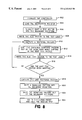
- FIG. 8 is a flow chart detailing the steps of the mission test execution step of the present invention shown in FIG. 6 .
- a boundary-scan IC chip 100 is shown in FIG. 1.
- a boundary register 102 is formed from a plurality of boundary register cells 104 .
- Each register cell 104 is disposed between an I/O terminal 106 ( a )-( b ) and the internal logic 108 of chip 100 .
- input terminals 106 ( a ) are shown on the left-hand side of chip 100
- output terminals 106 ( b ) are shown on the right-hand side of chip 100 .
- Some of the I/O terminals may be bi-directional.
- a scan path or scan chain 110 is formed through boundary register 102 .
- An IDCODE (i.e., identification) register 112 , a bypass register 114 , and an instruction register 116 are also included in chip 100 .
- IDCODE register 112 provides identification data for chip 100 .
- Bypass register 114 is a one-bit register which allows boundary register 102 to be bypassed.
- Instruction register 116 decodes instruction bits which are used to select test mode and also to control the operational mode of the chip during the test.
- a test access port (TAP) controller 118 is a state machine which controls boundary register 102 .
- Five I/O terminals have been added to chip 100 to accommodate boundary-scan. These five terminals constitute the test access port (TAP).
- a TDI (test data in) terminal provides serial test data and instruction bits to scan path 110 .
- a TDO (test data out) terminal provides serial output for scan path 110 .
- a TCK (test clock) terminal provides an independent test clock to chip 100 .
- a TMS (test mode select) terminal provides the logic levels needed to change the state of TAP controller 118 .
- a TRST (test rest) terminal is used to reset chip 100 .
- the TRST terminal shown in phantom, is optional.
- Circuit 200 includes six interconnected IC's U1-U6.
- Boundary register cells 104 are shown in each IC. Following convention, input cells are shown on the left-hand side of each IC, and output cells are shown on the right-hand side of each IC.
- Each pin of each IC is numbered consecutively from the lower left-hand corner and is referenced by that number along with the IC reference number. For example, U1-3 refers to pin 3 of U1.
- a scan path 110 is shown connecting register cells 104 of IC's U1-U6. Register cells 104 in scan path 110 form the boundary register ( 102 in FIG. 1 ).
- the TAP Controller is a sixteen-state state machine that controls each boundary scan IC chip 100 .
- the TAP Controller controls the shifting of test instructions and data bits into and out of chip 100 (FIG. 1 ).
- the TAP Controller state diagram illustrates general operation of boundary scan test circuitry.
- Each of the ICs connected in, for example, scan path 110 follow the same path through the TAP Controller state diagram. In other words, all the chips U1-U6 are in the same TAP state at any given time.
- the TAP Controller state diagram includes two columns with nearly identical labels for each position within the columns. Each position represents a state of the TAP Controller.
- the sixteen states vary only by the suffixes appended to the end of each state. The suffixes identify the column and register operation that they affect.
- DR is the data registers column.
- the states of the data registers are controlled by the states shown in this column.
- the data registers can be the Boundary Register, the Bypass Register, or the ID Register.
- IR is the instruction register column.
- the states of the instruction registers are controlled by the states in this column.
- the instruction register is a mandatory component of every boundary-scan device.
- a zero or a one is shown. These numbers indicate the bit state of the TMS input signal required to move from one state to the next.
- the TMS input signal controls the changing of states.
- the TAP Controller state diagram changes to the state indicated by the TMS value only during a rising edge of the test clock (TCK).
- TEST-LOGIC-RESET is the normal starting state of the device.
- the integrity of scan path 110 is tested prior to executing a mission test. This ensures that scan path 110 is in operational order and is not damaged. Scan path 110 may be damaged if, for example, a component in scan path 110 is dead or missing, a component in scan path 110 has a broken connection for one of its TAP pins, or a TDO to TDI connection between components is shorted to another node.
- the Instruction Registers of each IC chip U1-U6 must be programmed prior to performing the initial integrity test. Then, each IC chip U1-U6 in scan path 110 sets up a deterministic data pattern in its Instruction Register at CAPTURE-IR.
- a mission test is generated at step 404 , executed at step 406 and, thereafter, the results of the mission test are diagnosed at step 408 .
- the integrity test described above is performed on scan path 110 prior to mission test execution. This initial integrity test is run prior to execution of a mission and, generally, is only run once prior to plural mission tests. Thereafter, the integrity of scan path 110 , generally, is considered to be assured based on the initial integrity test. Accordingly, the test results of the mission test are considered to be reliable without further assurances and are summarily diagnosed at step 408 to obtain, ostensibly, reliable test diagnosis.
- FIG. 5 details the steps of the mission test execution step 406 shown in FIG. 4 .
- the TAP Controller is initialized to TEST-LOGIC-RESET. (See FIG. 3 for the diagram of the TAP Controller.)
- the Instruction Registers are loaded such that the boundary register is put between TDI and TDO for each IC.
- a test vector is serially shifted into the boundary register.
- the test vector is written to the test logic.
- a response pattern is captured (read) into the shift portion of the Boundary Registers.
- the captured response pattern is shifted out of the Boundary Registers while the next test vector is being shifted into the Boundary Registers.
- the next test vector is written to the test logic. If, at decision step 516 , the last test vector has been written to the test logic, then the last response pattern is captured at step 518 and written to the test logic at step 519 . If the last test vector has not been written to the test logic, then a response pattern is captured at step 510 . Finally, at step 520 , after all the response patterns have been captured, the mission test is stopped and returned to TEST-LOGIC-RESET, at step 520 . A more detailed discussion of the basic mission test execution steps is found in The Boundary - Scan Handbook at pp. 103-105.
- an initial integrity test is performed prior to mission test execution step 406 , the inventors recognize that it is possible that after the initial integrity test and/or during mission test execution, an operational flaw may occur in the IC chip 100 circuitry and cause the mission test to behave incorrectly.
- a mission test induced ground bounce may cause the injection of extra pulses on the TCK line which will cause an advance in TAP Controller 118 to an unexpected state.
- one or more of the ICs on the board may be at a different state than the other ICs.
- a timing condition e.g., a critical race
- TAP Controller may also cause improper state sequencing.
- the TMS line (which “steers” the transitions) is set to 1. If an extra TCK clock pulse occurs due to ground bounce, the result is to end up one state farther in the diagram, at state SELECT-IR-SCAN. The subsequent testing that wants to proceed one to CAPTURE-DR, etc, instead proceeds to CAPTURE-IR, etc.
- This has the effect of reprogramming the instruction register 116 of the effected IC chip 100 with random test data, which destroys the mission test setup. The net effect of this is that several IC chips 100 may “fall out” of their programmed test modes into some other instruction state.
- FIG. 2 shows a scan path 110 passing through the boundary register cells 104 of IC chips U1-U6. Accordingly, this scan path includes thirty-eight cells 104 representing thirty-eight bits. Thus, when a mission test is executed, the user relies on the configuration of scan path 110 remaining the same.
- scan path 110 is thirty-eight bits long
- the operator will serially shift the thirty-eight bit long test vector into the boundary register cells 104 expecting a thirty-eight bit response pattern to be shifted out. Accordingly, the operator, relying on the configuration of scan path 110 , simply identifies the next thirty-eight bits that are shifted out of scan path 110 to be the thirty-eight bit response pattern.
- IC chip U5 has been reconfigured such that scan path 110 passes through the one-bit Bypass Register rather than the eight boundary register cells, the response pattern will only be thirty-one bits long.
- the operator relying on the assumption that the configuration of scan path 110 is the same, simply takes the next thirty-eight bits shifted out of scan path 110 as the response pattern.
- the response pattern is only thirty-one bits.
- the thirty-eight bit response pattern is incorrect. Nonetheless, mission test diagnosis is performed on this inaccurate response pattern.
- the diagnostics may indicate that certain pins are open or shorted.
- one of the ICs 100 on the circuit board may have become reconfigured. Based on this inaccurate data or mission test result, an operator may be led to believe that something is seriously wrong with the circuit board. Accordingly, a low-skilled technician may be given a repair ticket to repair the board. However, the technician will be wasting time looking for problems which may not actually exist.
- the inventors have discovered that such problems can be avoided by checking the integrity of scan path 110 prior to mission test diagnosis. If the integrity of scan path 110 is found to have been compromised after the mission test is executed and prior to test diagnosis, then it is likely that something fairly sophisticated is wrong with the board. Thus, before mission test diagnosis is begun, the board can be sent to an engineering station for an engineer to determine why the integrity of scan path 110 has been compromised during test execution.
- FIG. 6 shows the steps in accordance with the invention for performing a mission test.
- a mission test is generated, at step 604 , by generating a plurality of mission test vectors.
- the mission test of the present invention is executed at step 606 , as discussed in the following and as shown in FIG. 8 .
- an initial integrity test is performed prior to test execution step 606 .
- steps 606 and 608 are depicted and discussed as separate steps, it is understood that parts of step 606 may overlap with parts of step 608 and vice versa.
- a post-mission test integrity check is performed at step 608 to assure the integrity of the executed mission test.
- This post-mission test integrity check of step 608 identifies whether scan path 110 has been reconfigured at some point after the initial integrity test or during mission test execution step 606 .
- an expected bit length is determined at step 702 .
- the expected bit length represents the quantity of bits in scan path 110 . This quantity is generally known or can be calculated. In particular, the expected bit length may be calculated by adding the bits in scan path 110 .
- An actual bit length of scan path 110 is determined at step 704 . How the actual bit length is determined is discussed in greater detail in the following discussion.
- the actual bit length represents the actual configuration of scan path 110 after the mission test has been executed.
- the actual bit length is compared with the expected bit length.
- An invalid mission test is indicated at step 708 if the actual bit length is not equal to the expected bit length.
- step 702 is shown to be performed prior to step 704 , step 702 may be performed at any point prior to the step 706 , which is when the expected bit length must be known so that the comparison between the expected bit length and the actual bit length can be made.
- Steps 802 , 804 , 806 , 808 , 810 , 812 , 814 , 816 , 822 and 824 are the same steps shown in FIG. 5 and discussed above. Accordingly, no further discussion is provided.
- the last captured response pattern is shifted out while a signature pattern is shifted into scan path 110 at step 820 .
- the signature pattern is shifted out of the scan path at step 822 .
- the circuit can proceed to TEST-LOGIC-RESET and halt the mission test at step 824 .
- the signature pattern may be shifted into the scan path 110 while shifting the last response pattern out. Then, the signature pattern is shifted out by shifting “don't care” or random bits into scan path 110 . However, it is within the scope of the invention to have the signature pattern shifted into scan path 110 independent of the last response pattern.
- FIG. 8 shows steps 820 and 822 at the end of the executed mission test, that is, after the last response pattern has been capture among a series of test vectors. However, it is within the scope of the invention to perform steps 820 and 822 after step 810 or 812 . Accordingly, steps 820 and 822 may be performed after every frame in the mission test or at the end of the entire mission test.
- the signature pattern is shifted in concurrently with the shifting out of the last test result of the mission test.
- the length of the scan path can be determined based on the number of clock cycles required to shift the signature pattern through the scan path. This is most readily accomplished by shifting the scan path a number of clock cycles equal to twice the expected length of the scan path. If the signature pattern is equal in length to the scan path, then this will result in the test pattern traveling through the scan path with the last bit exiting the scan path on the last clock cycle. The last n bits out the scan path should then match the n bits of the signature pattern (for an n bit long scan chain). If the bits of the pattern out do not match the bits of the pattern in, then the actual length of the scan path does not match the expected length.
- the signature pattern has a bit length equal to the expected bit length. If the actual bit length of scan path 110 is equal to the expected length of scan path 110 , then when the signature pattern is shifted into the boundary register cells 104 of scan path 110 , all the bits should be disposed in each of the boundary register cells 104 of scan path 110 . That is, none of the signature pattern bits should have been outputted.
- the signature pattern is shifted out by shifting a quantity of “don't care” bits (equal to the expected bit length or signature pattern bit length) into scan path 110 . If the signature pattern shifted out is not identical to the signature pattern shifted in, then scan path 110 has been reconfigured during mission test execution step 606 . If the signature pattern shifted out is identical to the signature pattern shifted in, then the configuration of scan path 110 has remained unchanged.
- FIG. 2 is referred to.
- “01001100011100001111000001111100001111” may be set up as the thirty-eight bit signature pattern (which is equal to the expected bit length of scan path 110 ). This signature pattern may then be shifted into the thirty-eight bit scan path 110 shown in FIG. 2 . When the entire signature pattern is shifted into the boundary register cells 104 of scan path 110 , each bit will occupy one of the boundary register cells 104 . The thirty-eight bit signature pattern is shifted out of scan path 110 as discussed above. If the configuration of scan path 100 has not been changed during mission test execution step 606 , then the output signature pattern will be identical to the input signature pattern.
- the compromised output signature pattern will not be identical to the input signature pattern.
- one of the IC chips such as U5 (FIG. 2) shifts over from the eight bit boundary register (as shown) to the one bit instruction register (not shown) then the bit length of scan path 110 has been reconfigured to a thirty-one bit length rather than the expected thirty-eight bit length.
- the output signature pattern will be compromised and will not be identical to the input signature pattern.
- the compromised output signature pattern will be “XXXXXX0100110001110000111100000111110”, where “X” is used merely as a means of representing the “don't care” bits.
- the signature pattern may be shifted in and out of scan path 110 as discussed above.
- the output of scan path 110 may be monitored for the presence of the signature bit pattern. Then, the response pattern of the mission test can be identified and distinguished from the signature bit pattern (on one end of the response pattern) and from the known bits (on the other end of the response pattern). Once the response pattern of the mission test is identified, then the bit length of the response pattern is counted to obtain the actual bit length of the scan path 110 .
- the signature pattern is shifted through scan path 110 independent of the response pattern and after test execution step 606 .
- the operator identifies “when” the bit pattern begins to shift out of scan path 110 to determine the actual bit length of scan path 110 after test execution. For example, a number of clock cycles TCK required to shift the bit pattern through scan path 110 is counted and compared.
- the configuration of scan path 110 has been compromised during test execution step 608 and an invalid test is indicated. Accordingly, a test operator will know that the scan path 110 has been reconfigured after test execution step 608 and will not proceed with test diagnosis until the integrity of scan path 110 is fixed and assured.
Abstract
Description
Claims (16)
Priority Applications (1)
| Application Number | Priority Date | Filing Date | Title |
|---|---|---|---|
| US08/370,076 US6243843B1 (en) | 1995-01-09 | 1995-01-09 | Post-mission test method for checking the integrity of a boundary scan test |
Applications Claiming Priority (1)
| Application Number | Priority Date | Filing Date | Title |
|---|---|---|---|
| US08/370,076 US6243843B1 (en) | 1995-01-09 | 1995-01-09 | Post-mission test method for checking the integrity of a boundary scan test |
Publications (1)
| Publication Number | Publication Date |
|---|---|
| US6243843B1 true US6243843B1 (en) | 2001-06-05 |
Family
ID=23458121
Family Applications (1)
| Application Number | Title | Priority Date | Filing Date |
|---|---|---|---|
| US08/370,076 Expired - Lifetime US6243843B1 (en) | 1995-01-09 | 1995-01-09 | Post-mission test method for checking the integrity of a boundary scan test |
Country Status (1)
| Country | Link |
|---|---|
| US (1) | US6243843B1 (en) |
Cited By (4)
| Publication number | Priority date | Publication date | Assignee | Title |
|---|---|---|---|---|
| US6581190B1 (en) * | 1999-11-30 | 2003-06-17 | International Business Machines Corporation | Methodology for classifying an IC or CPU version type via JTAG scan chain |
| US20030159096A1 (en) * | 2002-02-19 | 2003-08-21 | Balzer Raymond John | Boundary scan with ground bounce recovery |
| US6662327B1 (en) * | 1998-05-13 | 2003-12-09 | Janusz Rajski | Method for clustered test pattern generation |
| US20140059384A1 (en) * | 2012-08-22 | 2014-02-27 | Tektronix, Inc. | Test and measurement instrument with auto-sync for bit-error detection |
Citations (9)
| Publication number | Priority date | Publication date | Assignee | Title |
|---|---|---|---|---|
| US4764915A (en) * | 1982-01-12 | 1988-08-16 | Discovision Associates | Method and apparatus for recording a multiplexed signal on a record medium |
| US5027353A (en) | 1989-04-17 | 1991-06-25 | At&T Bell Laboratories | Method for testing interconnections |
| US5029166A (en) | 1989-05-31 | 1991-07-02 | At&T Bell Laboratories | Method and apparatus for testing circuit boards |
| US5130988A (en) | 1990-09-17 | 1992-07-14 | Northern Telecom Limited | Software verification by fault insertion |
| US5166937A (en) | 1990-12-26 | 1992-11-24 | Ag Communication System Corporation | Arrangement for testing digital circuit devices having tri-state outputs |
| US5172377A (en) | 1990-09-07 | 1992-12-15 | Genrad, Inc. | Method for testing mixed scan and non-scan circuitry |
| US5175494A (en) * | 1989-09-29 | 1992-12-29 | Kabushiki Kaisha Toshiba | Test simplifying circuit contained in digital integrated circuit |
| US5260649A (en) | 1992-01-03 | 1993-11-09 | Hewlett-Packard Company | Powered testing of mixed conventional/boundary-scan logic |
| US5270642A (en) * | 1992-05-15 | 1993-12-14 | Hewlett-Packard Company | Partitioned boundary-scan testing for the reduction of testing-induced damage |
-
1995
- 1995-01-09 US US08/370,076 patent/US6243843B1/en not_active Expired - Lifetime
Patent Citations (9)
| Publication number | Priority date | Publication date | Assignee | Title |
|---|---|---|---|---|
| US4764915A (en) * | 1982-01-12 | 1988-08-16 | Discovision Associates | Method and apparatus for recording a multiplexed signal on a record medium |
| US5027353A (en) | 1989-04-17 | 1991-06-25 | At&T Bell Laboratories | Method for testing interconnections |
| US5029166A (en) | 1989-05-31 | 1991-07-02 | At&T Bell Laboratories | Method and apparatus for testing circuit boards |
| US5175494A (en) * | 1989-09-29 | 1992-12-29 | Kabushiki Kaisha Toshiba | Test simplifying circuit contained in digital integrated circuit |
| US5172377A (en) | 1990-09-07 | 1992-12-15 | Genrad, Inc. | Method for testing mixed scan and non-scan circuitry |
| US5130988A (en) | 1990-09-17 | 1992-07-14 | Northern Telecom Limited | Software verification by fault insertion |
| US5166937A (en) | 1990-12-26 | 1992-11-24 | Ag Communication System Corporation | Arrangement for testing digital circuit devices having tri-state outputs |
| US5260649A (en) | 1992-01-03 | 1993-11-09 | Hewlett-Packard Company | Powered testing of mixed conventional/boundary-scan logic |
| US5270642A (en) * | 1992-05-15 | 1993-12-14 | Hewlett-Packard Company | Partitioned boundary-scan testing for the reduction of testing-induced damage |
Non-Patent Citations (10)
| Title |
|---|
| Cheng et al., "Diagnosis for Wiring Interconnects," 1990 Int'l Test Conf., 1990 IEEE, Paper 27.2, pp. 565-571. |
| Cheng et al., "Optimal Diagnostic Methods for Wiring Interconnects," 1992 IEEE Transactions on a Computer-Aided Design, vol. II, No. 9, Sep. 1992, pp. 1161-1166. |
| de Jong, "Boundary Scan Test Used at Board Level-Moving Towards Reality," 1990 Int'l Test Conf, 1990 IEEE, Paper 9.2, pp. 235-242. |
| Hansen, "Testing Conventional Logic and Memory Clusters Using Boundary Scan Devices as Virtual ATE Channels," 1989 Int'l Test Conf, 1989 IEEE, Paper 7.1, pp. 166-173. |
| Hassan et al., "Testing and Diagnosis of Interconnects Using Boundary Scan Architecture," 1988 Int'l Test Conf, 1989 IEEE, Paper 7.1, pp. 126-137. |
| Jarwala et al., "A New Framework for Analyzing Test Generation and Diagnosis Algothrithms for Wiring Interconnects," 1989 Int'l Test Conf, 1989 IEEE, Paper 3.3, pp. 63-70. |
| Kashiwabara et al., "Permutation Layout With Arbitrary Between-pins Capacities," 1990 IEEE, pp. 340-343. |
| McBean et al., "Bridging Fault Algorithms for a Boundary Scan Board," pp. 6/1-6/8. |
| McBean et al., "Testing Interconnect: A Pin Adjacency Approach," 1993 IEEE, pp. 484-490. |
| Yau et al., "A Unified Theory for Designing Optimal Test Generation and Diagnosis Algorithms for Board Interconnects," 1989 Int'l Test Conf, 1989 IEEE, Paper 3.4, pp. 71-77. |
Cited By (8)
| Publication number | Priority date | Publication date | Assignee | Title |
|---|---|---|---|---|
| US6662327B1 (en) * | 1998-05-13 | 2003-12-09 | Janusz Rajski | Method for clustered test pattern generation |
| US6581190B1 (en) * | 1999-11-30 | 2003-06-17 | International Business Machines Corporation | Methodology for classifying an IC or CPU version type via JTAG scan chain |
| US20030159096A1 (en) * | 2002-02-19 | 2003-08-21 | Balzer Raymond John | Boundary scan with ground bounce recovery |
| GB2385936A (en) * | 2002-02-19 | 2003-09-03 | Agilent Technologies Inc | Boundary scan test with ground bounce recovery |
| GB2385936B (en) * | 2002-02-19 | 2005-05-18 | Agilent Technologies Inc | Boundary scan with ground bounce recovery |
| US7107503B2 (en) * | 2002-02-19 | 2006-09-12 | Agilent Technologies, Inc. | Boundary scan with ground bounce recovery |
| US20140059384A1 (en) * | 2012-08-22 | 2014-02-27 | Tektronix, Inc. | Test and measurement instrument with auto-sync for bit-error detection |
| US8793536B2 (en) * | 2012-08-22 | 2014-07-29 | Tektronix, Inc. | Test and measurement instrument with auto-sync for bit-error detection |
Similar Documents
| Publication | Publication Date | Title |
|---|---|---|
| Mitra et al. | X-compact: An efficient response compaction technique | |
| US7574644B2 (en) | Functional pattern logic diagnostic method | |
| US5497378A (en) | System and method for testing a circuit network having elements testable by different boundary scan standards | |
| Lala | An introduction to logic circuit testing | |
| JP4055980B2 (en) | Digital circuit test equipment | |
| US5682392A (en) | Method and apparatus for the automatic generation of boundary scan description language files | |
| US7010735B2 (en) | Stuck-at fault scan chain diagnostic method | |
| US7039845B2 (en) | Method and apparatus for deriving a bounded set of path delay test patterns covering all transition faults | |
| EP0834081A1 (en) | Method and apparatus for testing a megacell in an asic using jtag | |
| US4996691A (en) | Integrated circuit testing method and apparatus and integrated circuit devices for use therewith | |
| US6173428B1 (en) | Apparatus and method for testing using clocked test access port controller for level sensitive scan designs | |
| US6178534B1 (en) | System and method for using LBIST to find critical paths in functional logic | |
| US6058255A (en) | JTAG instruction decode test register and method | |
| Cantoro et al. | Automatic generation of stimuli for fault diagnosis in IEEE 1687 networks | |
| Kochte et al. | Test strategies for reconfigurable scan networks | |
| US5550841A (en) | Method for failure analysis of megachips using scan techniques | |
| CN100370430C (en) | Boundary Scanning chain self-testing method | |
| US6243843B1 (en) | Post-mission test method for checking the integrity of a boundary scan test | |
| Wang et al. | A self-test and self-diagnosis architecture for boards using boundary scans | |
| Maunder et al. | An introduction to the boundary scan standard: Ansi/ieee std 1149.1 | |
| KR100694315B1 (en) | At-speed interconnect test controller for system on chip using multiple system clock and having heterogeneous cores | |
| Tekumalla | On reducing aliasing effects and improving diagnosis of logic BIST failures | |
| KR20060055595A (en) | Simplification apparatus of test access port for chip test | |
| JPH06213972A (en) | Boundary scan cell circuit, boundary scan test circuit and their using method | |
| Haider et al. | The split boundary scan register technique for testing board interconnects |
Legal Events
| Date | Code | Title | Description |
|---|---|---|---|
| AS | Assignment |
Owner name: HEWLETT-PACKARD COMPANY, CALIFORNIA Free format text: ASSIGNMENT OF ASSIGNORS INTEREST;ASSIGNORS:PARKER, KENNETH P.;ORESJO, STIG;REEL/FRAME:007597/0694;SIGNING DATES FROM 19941222 TO 19941223 |
|
| AS | Assignment |
Owner name: HEWLETT-PACKARD COMPANY, COLORADO Free format text: MERGER;ASSIGNOR:HEWLETT-PACKARD COMPANY;REEL/FRAME:010759/0049 Effective date: 19980520 |
|
| AS | Assignment |
Owner name: AGILENT TECHNOLOGIES INC, CALIFORNIA Free format text: ASSIGNMENT OF ASSIGNORS INTEREST;ASSIGNOR:HEWLETT-PACKARD COMPANY;REEL/FRAME:010977/0540 Effective date: 19991101 |
|
| STCF | Information on status: patent grant |
Free format text: PATENTED CASE |
|
| FPAY | Fee payment |
Year of fee payment: 4 |
|
| FPAY | Fee payment |
Year of fee payment: 8 |
|
| FPAY | Fee payment |
Year of fee payment: 12 |
|
| AS | Assignment |
Owner name: KEYSIGHT TECHNOLOGIES, INC., CALIFORNIA Free format text: ASSIGNMENT OF ASSIGNORS INTEREST;ASSIGNOR:AGILENT TECHNOLOGIES, INC.;REEL/FRAME:033746/0714 Effective date: 20140801 |