US4901064A - Normal vector shading for 3-D graphics display system - Google Patents
Normal vector shading for 3-D graphics display system Download PDFInfo
- Publication number
- US4901064A US4901064A US07/117,162 US11716287A US4901064A US 4901064 A US4901064 A US 4901064A US 11716287 A US11716287 A US 11716287A US 4901064 A US4901064 A US 4901064A
- Authority
- US
- United States
- Prior art keywords
- vector
- command
- processor
- pixel
- input data
- Prior art date
- Legal status (The legal status is an assumption and is not a legal conclusion. Google has not performed a legal analysis and makes no representation as to the accuracy of the status listed.)
- Expired - Fee Related
Links
Images
Classifications
-
- G—PHYSICS
- G06—COMPUTING; CALCULATING OR COUNTING
- G06T—IMAGE DATA PROCESSING OR GENERATION, IN GENERAL
- G06T15/00—3D [Three Dimensional] image rendering
- G06T15/50—Lighting effects
- G06T15/506—Illumination models
Definitions
- This invention relates to graphics display systems, and in particular, to a system for specifying the color and intensity of pixels in an image to be displayed on such systems.
- Three-dimensional computer graphics displays are used to display images to a user as if he were observing a real world environment. These systems store in a data base a representation in three-dimensional coordinates of three-dimensional objects, as well as information concerning their color and other properties. Additional "environment" information including the number, color, location, and other properties of illumination sources, atmospheric properties, and many other details also may be specified.
- the display is generated after being provided with the desired viewing angle for the viewer.
- the user may specify the field of view, the size of the image to be produced, and the back plane of the viewing volume so as to include or eliminate background as desired.
- the system must calculate all the details of the image, including determining which objects obscure others from the viewer's point of view, and present them accordingly.
- the image data base in a typical graphics display system stores a description of each object in a scene as a number of small polygons which cover the surface of the object in the same manner that a number of small tiles can cover a wall or other surface.
- Each polygon is described by a list of its vertex coordinates (X, Y, Z) and a specification of material surface properties (e.g., color, texture, shininess, etc.), as well as possibly the normal vectors to the surface at each vertex.
- the polygons in general are triangles or quadrilaterals (which can be decomposed into pairs of triangles).
- a transformation engine transforms the object coordinates in response to the angle of viewing selected by a user.
- a clipping circuit eliminates the triangles which are outside the viewing area and "clips" the polygons which are partly inside and partly outside the viewing area.
- the vertices of the resulting polygons are transmitted by the clipping circuit to the next stage in coordinates corresponding to the viewing screen (X, Y coordinates) with an associated depth for each vertex (Z coordinate).
- a lighting model 20 is applied next to specify the color of each triangle. Then the triangles with their color values are transmitted to a rasterizer.
- the rasterizer determines which pixel positions are covered by that triangle and compares the depth values (Z) for the polygon being processed with the depth value of any pixel which already in the frame buffer. If the depth value of the new polygon pixel is smaller, indicating that it is in front of the polygon already written into the frame buffer, then the new value replaces the value in the frame buffer. This process is repeated until all polygons have been rasterized. Then the video controller displays the contents of the frame buffer on a display a scan line at a time in raster order.
- the basic method is characterized by a single rasterization processor writing pixels one by one into a frame buffer.
- the improved systems are characterized by employing a large number of processors in parallel in which the individual processors represent pixels in the frame buffer. These systems differ in how the processors are assigned to pixels.
- pixel-planes method employs brute force and assigns a processor for every pixel in the display screen. See, for example, Foulton, et al., Pixel Planes: Building a VLSI-Based Graphics System, 1985 Chapel Hill Conference on Very Large Scale Integration 35 (H. Fuchs ed., 1985).
- the edges are two-dimensional polygon descriptions are sent one by one to the pixel processors.
- the processors determine which side of each edge the pixel they represent is on, and consider themselves inside a particular polygon only if they are on the correct side of all its edges. Next, if the depth information is less than that of any previously stored pixel value, the pixel processors load interpolated depth and color information into their pixel value registers.
- Scan Line Access Memory requires custom storage registers for each pixel in the display, but only contains enough pixel processors for a single scan line.
- Scan Line Access Memory requires custom storage registers for each pixel in the display, but only contains enough pixel processors for a single scan line.
- Such a system is described in Demetrescu, High Speed Image Rasterization Using Scan Line Access Memories, 1985 Chapel Hill Conference on Very Large Scale Integration 35 (H. Fuchs ed., 1985).
- External rasterization hardware breaks each polygon into horizontal runs of pixels. Only the start and stop addresses of these runs are entered into the SLAM chips, and the internal one-dimensional array of pixel processors determines which pixels are covered by this run. The results are written into an on-chip memory array, indexed by the y location of the particular run.
- the super buffer also employs a single scan line of pixel processors, but does not require local memory for all the pixels effected by them to be on the same chip.
- This system is described in Gharachorloo and Pottle, Super Buffer: A Systolic VLSI Graphics Engine for Real Time Raster Image Generation, 1985Chapel Hill Conference on Very Large Scale Integration 35 (H. Fuchs ed., 1985).
- the previous two systems take input polygons one at a time, rasterizing each one completely before going on to the next.
- the super buffer requires all the polygons to be displayed to be presorted by the y scan line on which they first appear. Each polygon is broken into runs on a scan line basis and the runs sent to the pipe of pixel processors.
- This invention provides a high speed technique for coloring pixels in a 3-D graphics display system.
- Parameters of a lighting model are loaded into a pipeline chips fabricated according to the invention.
- streams of surface normal pixels are subjected to the lighting model, producing a stream of color values for image pixels is provided as a final output.
- Each chip fabricated according to the technique of the invention contains all of the hardware necessary to perform a complete shading calculation every 64 clock cycles and initiate a new shading calculation every 16 cycles. By placing 16 chips in series, a pipeline is formed which is capable of applying the lighting model continuously at 20 megaHertz.
- the system for determining the color of a plurality of pixels includes a series of memories for storing a lighting model, an input section connected to receive data indicative of at least a normal vector for each of the pixels in turn, and a plurality of interconnected processors connected to the input and to the storage elements, for applying the lighting model to a pixel using the normal vector.
- the invention also includes a technique for assigning individual pixels to individual processors for application of the lighting model.
- the system receives the normal vector for each pixel to be shaded, its Z depth, and information about the material characteristics represented by the pixel.
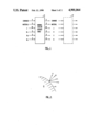
- FIG. 1 is a diagram showing the overall functionality of the normal vector shading system of this invention
- FIG. 2 illustrates the geometry of the lighting model employed
- FIG. 3 is a more detailed block diagram of the normal vector shading system.
- a perspective projection is generated with hidden surfaces removed, and then shading and color patterns are applied to the visible surfaces.
- a shading model is used to calculate the intensity of light for each portion of the surface of the displayed object. The intensity calculation for each portion of the object is based upon the optical properties of the surface at that location, its relative position with respect to other surfaces, and its orientation with respect to the light source or sources.
- One now well known technique for shading objects was developed Phong Bui Tuong.
- the normal vector shader system of this invention employs Phong shading of colored materials by multiple light sources, which themselves may be colored.
- FIG. 1 shows the overall functionality of a preferred embodiment of the normal vector shader system (sometimes referred to herein as "NVS system”).
- NVS system normal vector shader system
- This system is intended to be employed in conjunction with U.S. Ser. No. 117,111 filed on 11/4/87, entitled “3D Graphics Display System Using Triangle Processor Pipeline,” and U.S. Ser. No. 117,110 filed on 11/4/87, entitled, "Triangle Processor for 3D Graphics Display System.”
- An NVS chip 10 receives data representing surface normal vectors NX, NY and NZ with associated depth Z in the image for that normal vector, together with information about the material properties at that point. Command information is also supplied to the NVS 10.
- the system passes the command, material, and Z-depth information through unaltered, but supplies complete color information in a red-green-blue system with 8 bits representing the intensity of each of the three colors.
- RGB Red-green-blue
- other color systems and digital word lengths may be employed.
- a second NVS chip 10' is also shown in FIG. 1 to illustrate how a series of such chips may be interconnected in a pipeline.
- the first chip will process the first pixel, while the second chip processes the second pixel, etc.
- a pipeline of 16 chips is employed with each chip processing every 16th pixel.
- FIG. 2 displays the geometry of the lighting model.
- N is the vector normal to the surface of a displayed object 15
- V is the viewpoint normal vector
- L is the light source vector
- R is the reflectance of the viewpoint vector through the surface normal vector.
- all of the vectors are expressed in coordinates referenced to a fixed universal coordinate system, herein termed "world coordinates," as opposed to coordinates referenced to the portion of the object being displayed.
- the viewpoint vector is not constant across the entire screen, but is interpolated to point at each pixel in turn. Additionally, in the case of multiple light sources, there will be a different vector L for each light source.
- the ambient illumination due to light source l on a patch of material m is:
- MC[m] is from a writable table of 128 different material colors broken up into RGB components: MC[m] ⁇ r, MC[m] ⁇ g, and MC[m] ⁇ b;
- LA[l] is from a writable table which allows specification of the amount that a particular light source adds to the ambient illumination
- LC[l] is from a writable table of 5 light colors divided into components LC[l] ⁇ r, LC[l] ⁇ g, and LC[l] ⁇ b.
- the diffuse illumination due to light source l on a patch of material m is:
- LN[l] is from a writable table of 5 light source normal vectors divided into components LN[l] ⁇ X, LN[l] ⁇ Y, and LN[l] ⁇ Z.
- the specular component is:
- POW[s][n] is from a table of precomputed specularity power functions.
- the second index selects 1 of 12 predetermined powers to which to raise the 8-bit input.
- the powers chosen will be in the range of 1 to 60;
- W[i][n] is one of four preprogrammed specular reflection functions available for different material types. These allow the angle between the normal and the light source to affect the intensity of the specular component;
- SP[m] is from writable table of 128 different 4-bit specular powers indices for materials
- SF[m] is from writable table of 128 different 2-bit specular reflection function indices for materials
- SI[m] is from writable table of 128 different 5-bit specular intensity fractional multipliers for materials.
- the final RGB value for the shading prior to the Z-fade stage is given by one of the four equations below, depending upon the condition described:
- this pixel is a background pixel, it does not belong to any triangle, and the command supplied with the normal vector will cause the RGB value to default to one of the two background colors, dependent upon the sign of z component of V Vy.
- a positive Vy indicates a "sky” pixel, a negative Vy indicates a "ground” pixel:
- BC is one of two default background colors, with RGB components: BC[i] ⁇ r, BC[i] ⁇ g, and BC[i] ⁇ b.
- the effects of all the light sources can be modeled by summing together the appropriate one of the above equations over 1, but excluding the contribution of any light source for which LE[m]is 0.
- LE[m] is taken from a writable table of 128 different 5-bit light source enable bits, 1 bit for each light source, indexed by material.
- the background color can be bled into object pixels as a function of Z as follows. First the percentage fade r is calculated: If Z is in front of Pf:
- the normal vector shader is embodied on a single integrated circuit.
- a plurality of serially connected chips are employed in the system with lighting model parameters being loaded into the pipeline. Then rasterized streams of surface normal pixels are subjected to the illumination model producing a stream of 24-bit RGB image pixels as an output.
- Each normal vector shader chip in the pipeline contains all the circuitry necessary to perform effectively a complete shading calculation every 16 clock cyles.
- a pipeline is formed which is capable of applying the lighting model continuously at 20 megaHertz.
- the resulting 16-chip subsystem forms a complete 5-light source Phong shading on each individual pixel of the scene at 20-megapixel-per-second data rates. This provides a substantial speed advantage over all previously existing implementations of sophisticated lighting models.
- Each normal vector shader chip responds to RAZ and RAZD commands which are produced by the triangle processor chips (see. Ser. No. 117,110, cited above.)
- the RAZ command indicates that a pixel has passed through the triangle processor pipeline without being obscured by any active triangles and that a background shading calculation should be performed to generate an RGB-Z value.
- the RAZD command indicates that a real normal vector is present and that pixel is to be shaded using the lighting model.
- the series of normal vector shader chips are designed to abut each other, and accordingly the input and output pins are provided in complementary pairs, and the pin-outs match those of the triangle processor.
- the functional input/output diagram for an individual chip is shown in FIG. 1.
- the chip accepts data representing the surface normal vectors NX, NY, and NZ with associated Z depth and material index.
- the chip sends out data representing illuminated surface RGB colors with associated Z depth and material index.
- Each chip includes an input buffer 20 and an output buffer 24 to interface that chip with other chips in the pipeline of an overall graphics processing system. To reduce pin count the input signals to the chip are multiplexed by double clocking.
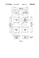
- FIG. 3 is a more detailed diagram of a normal vector shader chip.
- the normal vector shader chip includes a number of banks of externally-loadable registers for storing three major types of information--light sources, a viewpoint vector, surface material properties--as well as additional registers for storing miscellaneous values. Table I below is a list of the registers.
- the names of the registers are set forth in Table I together with the number of bits which specifies the physical size of the register.
- the column labeled "Number of Bits/Component" specifies for each vector type the size of each component.
- the type column identifies whether the register itself comprises an array of registers. All of the registers are implemented using static memory to eliminate the need for refreshing their contents.
- the normal vector shader chip supports five light sources of any color, with fewer than five light sources obtainable by setting the color of undesired lights to black.
- more or fewer light sources can be employed.
- the first parameter is a normal vector pointing in the direction of the light source.
- the second parameter is the RGB color of the light source normalized as necessary depending upon the number of light sources for the scene.
- the third parameter is the ambient component of the light source, which is the fraction that an individual light source adds of its color to the illumination of portions of objects which are not visible to that light source.
- the fourth parameter is the diffuse component of that light source, and to allow for spot lighting this component may be disabled by the user. Because the normal vectors are specified in world coordinates, the light sources need not be specified every time the viewpoint changes and thus are set until the light sources are changed.
- the light normal register consists of five 27-bit registers representing a normal vector pointing in the direction of the infinite light source. Nine bits of each 27-bit register are used for the value of the X coordinate, 9 bits for the Y coordinate, and 9 bits for the Z coordinate.
- the five light color registers represent the RGB color of the illumination source.
- Each register includes three 8-bit fields, each field representing an unsigned number between 0 and 255, with 0 representing zero intensity on that color channel and 255 representing full intensity.
- the five light ambient registers represent the percentage of the light source color to illuminate portions of surfaces which are back facing with respect to the light source vector and thus do not receive direct illumination.
- each light source with its own ambient coefficient, allowance is provided for the selective sensitivity of the materials to differing light sources.
- a zero in the register corresponds to 0% sensitivity, while 255 in the register corresponds to 100% sensitivity.
- Table I also lists three of the viewpoint registers of viewpoint unit 30.
- the lighting model employed in the normal vector shader system does not assume that the viewpoint vector from the eye position to the surface of objects is constant. Instead, the viewpoint vector is tracked across the entire image with a separate viewpoint vector computed for each pixel in the image. This incremental computation is set up as a linear interpolation of an unnormalized vector across the face of a rectangle inscribed within a unit sphere. The head of the unnormalized viewpoint vector touches points on the rectangle corresponding to pixels on the screen. Before each vector is used in the lighting model, it is normalized to correct the vector to be a unit vector. The lighting model assumes all vectors are unit vectors. Once normalized the vector is stored within the viewpoint register 30 shown in FIG. 3. The viewpoint unit contains nine viewpoint registers as well as all circuitry necessary to interpolate the viewpoint vector across the image.
- the viewpoint vector is interpolated across the entire image, it is represented to a high accuracy by employing 24 bits for each of the X, Y, and Z coordinate components. Because of the number of bits employed, each vector component is loaded as a separate word, and thus, the three viewpoint vector registers require 9 cycles to load.
- viewpoint vector interpolator is determined by the field of view of the image, the aspect ratio of the image, the aspect ratio of the pixels, the number of pixels in each of X and Y directions, and the direction of view.
- the left v register itself includes three 24-bit registers, one for each of the X, Y, and Z directions.
- the three registers together initially represent a vector pointing from the eye position to one of the first 16 pixels (assuming a pipeline of 16 NVS chips is employed) on the uppermost scan line of the screen.
- the left v vector has a different initial value in each of the 16 chips in the pipeline.
- the left v vector is used as the starting value for the span v vector for its interpolation across the scan line.
- the left v vector register is incremented by the value of the yinc v vector register, causing the left v vector register to now point to the left-hand pixel on next scan line down from where it was before.
- the numeric range of the left v register is interpreted as a fraction between -1 and +1.
- the xinc v register also comprises three 24-bit registers, one for each of the X, Y, and Z components of the xinc v vector. These three registers together represent the vector necessary to increment the viewpoint vector from pointing at one pixel on the screen to pointing to the 16th pixel (assuming a pipeline of 16 NVS chips) to the right on the same scan line.
- the xinc v vector register is repeated added to the span x vector register when processing an image, thereby interpolating the span x from its initial value of left x to finally point to the last pixel on the right of the scan line.
- the yinc v register also comprises three 24-bit registers and represents the vector necessary to increment the left v viewpoint vector from pointing at a pixel on the left-hand edge on the screen to pointing at the appropriate one of the first 16 pixels on the next scan line down.
- Each 42-bit material register within SRAM 35 contains custom properties for that material.
- the system provides for up to 127 different materials to be represented in a single image frame.
- 24 bits of RGB color are provided by three 8-bit fields. This is the color value employed in the lighting model when pixels of this material are shaded.
- Each material register also includes 4 bits for selecting 1 of 12 different specularity powers. This value determines the amount of specular illumination present at a particular pixel, and generally corresponds to the shininess of the material.
- the material registers also include 5 bits of specularity intensity control. In addition to the power of specularity, this value is a fractional multiplier of the degree of specular contribution to pixel intensity.
- the material register also includes 2 bits for selecting 1 of 4 different incident angle dependent surface reflection coefficient tables. This is a further down multiplier of the amount of specular contribution of the output intensity. This value is based upon the angle between the normal to the surface and normal to a particular light source. Five bits of the material register enable the material to be sensitive to any combination of the five light sources. Two bits of each material register are employed by other circuitry outside of the normal vector shading system.
- Each of the sky and ground color registers includes three 8-bit fields to provide RGB information on the sky color and ground color used as background for the display image. Any pixel not otherwise employed in the displayed image will default to one of these two colors.
- the sky color is also the color toward which the depth cueing fades pixels which are to appear more distant from the viewer.
- the lighting model chooses between the sky color and ground color for unclaimed pixels by inspecting the sign of the viewpoint vector y component value. Positive values indicate that the vector from the eye position through that pixel is pointed toward the sky, rather than the ground. Negative values indicate the reverse.
- the ground plane effect may be disabled by setting both the sky color and the ground color to the same value. Alternatively, all background color may be disabled by setting the registers to the black level values.
- the configuration register is employed when a pipeline of normal vector shader chips are used.
- the configuration register configures a particular chip to a specified position within the pipeline as indicated by the data in the field.
- One bit of the configuration register is used as an enable bit to enable the chip to process any commands received by it. This bit allows one or more chips to be mapped out of the pipeline for testing or redundancy purposes.
- the ENABLE command sets the enable bits on all chips to which it is addressed.
- the IDLE command is effectively a no operation command. It is employed by other parts of the system to insert delays between commands or data if extra time is needed. Any data present on receipt of an IDLE command is passed through without alteration.
- the NEW command is employed by the triangle processor described in the above-referenced application, and has no effect on the shading chip.
- the SOL command precedes rasterization of a scan line and is ignored by the shader chip.
- the RAZ command discussed briefly above, indicates that a pixel has been completely processed by the triangle processor without being obscured by any active pixel, and thus the shading calculation for the background color is performed to generate an appropriate RGB-Z value.
- the RAZD command when received by the normal vector shader chip indicates that a real normal vector is present and a pixel is to be shaded using the lighting model.
- the EOL command indicates that rasterization has been completed for a given scan line. This command is employed by the chip to initiate the Y increment of the viewpoint vector interpolation.
- the NVS-LD command provides a means for loading all user programmable registers of the chip. Of the 60-bit word, the first 4 bits are the command, and the next 10 bits are the register address. The remaining bits are the data to be loaded into the register. The particular use of this command is discussed further below.
- the EX MAT command provides a mechanism for extending the limited material color RAM 35 on the shader chip.
- all RAZD pixels are directly followed by an EX MAT command having a data value to be used in place of the value stored in the material look-up table.
- This mechanism allows appending full 24-bit RGB color values to each RAZD command, thereby allowing the material color across the surface of a displayed triangle to be specified on a pixel-by-pixel basis.
- the EX MAT command may also provide data about the specular power coefficient or other material characteristics.
- the GRABBED command is employed when a chip diverts an input pixel to its internal shading process. When this occurs the chip substitutes a GRABBED command in place of the pixel, and this command passes down the pipeline to the remaining chips. Whenever a subsequent chip receives a GRABBED command, it knows that a chip further up the pipeline has taken a pixel for processing. This allows each chip to determine when it is appropriate for that chip to accept another pixel for processing by counting the number of commands which pass in the interim. If that chip has completed its computation, it will substitute its output for the GRABBED command.
- the shader chip accepts the output from the triangle processor chip, applies its lighting model, and generates a stream of RGB pixel values as output.
- the chips function as follows.
- the input signal to the pipeline is a stream of RAZ or RAZD pixels supplied by the triangle processors, with no gaps or other pixel types intermingled.
- the pipeline is empty, and upon receipt of the first pixel, the first shader chip will accept the data and supply a GRABBED command in place of the command received.
- the chip then begins performing a shading computation on the data received.
- Each pixel requires 64 cycles to complete, however, after the chip can begin processing another pixel.
- the first chip will still be processing the first pixel, and accordingly the first chip will pass that second pixel unaltered to the second NVS chip.
- the second chip accepts that data, substitutes a GRABBED command, and begins processing.
- the first chip After 16 such cycles, all 16 chips will have started processing pixels. Upon receipt of the 17th pixel, the first chip will have another window opened for beginning a shading calculation, and will again pass on a GRABBED command. Only after 64 pixels have entered the pipeline will the first chip complete transforming the first pixel's normal vector information into the first RGB pixel. When the first chip accepts the 65th pixel, rather than supplying a GRABBED command, it will send out an RGB command with the completed RGB data. This is passed through, without modification, all of the downstream NVS chips to emerge as the first output RGB value. The second chip acts in the same manner with respect to the 66th pixel, supplying as output the second RGB pixel. This process continues, resulting in a continuous stream of RGB data at the output pin of the 16th chip.
- FIG. 3 is a block diagram of the shader chip showing major functional units.
- Each NVS chip also includes a dot product unit 40 which accepts as input two 27-bit vectors and produces a single 9-bit signed result.
- a scaler-vector unit 44 accepts as input three 27-bit vectors, and in response multiplies the components of the first vector by the second, adds the components of the third vector, and produces a 27-bit vector result.
- a square root ROM 48 contains an inverse square root look-up table of 256 ⁇ 8.
- the square root ROM accepts as input a result from the dot product unit, and supplies as output the reciprocal of the square root of the input value.
- the output signal from the square root ROM is always supplied to the scaler vector unit 44 to normalize the vector.
- the specularity ROM 51 is 4096 ⁇ 8 and contains sixteen 256 ⁇ 8 look-up tables. Twelve of these tables contain power functions for different degrees of specularity, while the remaining four contain preprogrammed specular reflection functions for different types of material.
- the specularity ROM 51 contains both the specular reflection function data and specularity power function data. Both data tables have similar access patterns.
- the 256x8 bank is selected by the material RAM output register bits while the word within the bank is selected by the output from the dot product unit 40.
- the material SRAM 35 contains a 128 ⁇ 42 bit material property look-up table. Addressed by material index, each 42-bit word contains RGB colors of materials, the degree of specularity, and all the other material properties described in the lighting model.
- Multiplier-adder 54 is a 9 ⁇ 9 signed two's complement multiplier and adder. It accepts as input signals three 9-bit scalers, and in response, generates a 9-bit scaler result
- control unit 60 contains the microcode sequencer for the operation of the overall chip and is coupled to all of the other units.
- the shading chip is loaded within initial data using the NVS LD command.
- the load command consists of a 60-bit word with the four least significant bits being the command, and the next ten least significant bits being the register bits. The remaining 46 bits are used for data to be loaded into the addressed internal register. Of course, for most registers not all of the 46 bits are employed. Because the commands are essentially independent, the data may be loaded into the chip in any order as long as the pipeline is empty of pixel data. Thus, for example, the material SRAM 35 may be loaded in one block of 127 load commands, or individual entries modified one at a time. Because each NVS chip passes load commands on to the next chip in the pipeline without alteration, all load commands are executed by all of the chips in the pipeline.
- the one instance in which the load commands may not be entered in any order relates to the viewpoint unit 30.
- a special load sequence is required. This sequence consists of 16 load commands in a row, with each command specifying a left v vector register in the address field.
- each load command contains a special 4-bit idle count field loaded with 15 in the first load command, 14 in the next, etc. In this manner the first chip in the pipeline will execute the first of the 16 load commands and ignore the next 15. The second chip in the pipeline will never receive the first load command, instead receiving an IDLE command. It thus will execute the second load command and ignore the next 14.
- the shader chip as exemplified by the block diagram of FIG. 3 receives as input signals from the triangle processor chips the material index, the Z depth, and data representing the surface normal vector. All of the other necessary parameters are assumed to have been preloaded into the chip.
- the chip begins by computing light source independent information.
- the internally interpolated viewpoint vector from viewpoint unit 30 is normalized and restored in unit 30. This operation is performed by the dot product unit 40 in conjunction with the square root ROM 48 and the scaler-vector 44.
- pseudo-code Expressed in pseudo-code:
- the reflectance vector R is computed using the dot product unit 40 and scaler vector multiply and add unit 44.
- the vector products of the light source, the normalized surface normal vector, and the normalized reflectance vector are computed, again employing the dot product unit 40.
- the specular component is computed using the vector product computed above as an index into the specularity ROM 51.
- the results are multiplied together using multiplier 54 to provide a measure of the intensity per unit area of the surface being shaded.
- the ambient component resulting from surrounding surfaces, is then added to the diffuse component,
- the final RGB value may be computed by multiplying in the color of the material, its specular component, and multiplying by the light color:
- oRGB is the summation input for the RGB value computed for the previous light source, or 0 if this is the first light source.
- Mb is the slope of the fade relationship between the planes. Then, the background contribution bRGB is computed using:
- the light source dependent information is calculated once for each of the five different light sources, then summed to provide the final color value for that pixel. Any RGB overflows (over 255) are truncated to 255.
Abstract
Description
ambient=MC[m]* LA[l]* LC[l] (1)
R=2* (N·V) * N-V (3)
specular=POW[R·LN[l]][SP[m]]W[N·LN[l]][SF[m]]* SI[m]* LC[l ] (4)
RGB=MC[m]*LA[l]*LC[l] (5)
RGB=N (7)
RGB=BC[sign of Vy] (8)
r=Sf (9)
r=Sb (10)
r=Sb+(Z-Pb)*MB (11)
RGB=r*RGB+(1-r)*BC[0] (12)
              TABLE I
______________________________________
NVS REGISTER MAP
Register              Bits/
Name           Bits   Component Type
______________________________________
Material
        mat        42     varies  array of 128
Register:                         colors & props
Light   light normal
                   27     9       array of 5 vectors
Source  light color
                   24     8       array of 5 RGB
Registers:                        colors
        light ambient
                   8      8       array of 5 scaler
                                  ambient
                                  coefficients
Viewpoint
        left v     72     24      single vector
Registers:
        xinc v     72     24      single vector
        yinc v     72     24      single vector
Misc.   config.    16     16      control
Registers:
        sky color  24     8       single color
        ground color
                   24     8       single color
______________________________________
              TABLE II
______________________________________
NORMAL VECTOR SHADER COMMANDS
Command    Binary        Semantics
______________________________________
RESET      0111          Reset NVS
ENABLE     0110          Enable NVS
IDLE       0000          Idle cycle
NEW        0001          New triangle data
SOL        0100          Header for new line
EOL        0101          End of line
RAZ        0011          Rasterize
RAZD       0010          Rasterize + Data
RGB        1000          RGB output pixel
NVS LD     1001          NVS reg load
EX MAT     1010          External material
GRABBED    1011          Taken pixel
EXT        11xx          External command
______________________________________
temp=V'<dot>V'
temp=SQROM(temp)
V=temp <sv+>V'+0
temp=N'<dot>N'
temp=SQROM(temp)
N=temp<sv+>N, +0
cos nv=N<dot>V
R=(2*cos nv)<sv+>N-V
cos.sub.-- nl=LN[l]<dot>N
cos.sub.--rl=LN[l]<dot>R
temp=PWROM[SF[m]][cos.sub.--nl]
temp2=PWROM[SP[m]][cos.sub.--rl]
temp=temp <*>temp2
spec=temp <*>SI[m]
da=cos.sub.-- nl +LA[l]
temp=CM[m]<sv+>da +spec
oRGB=CL[l]<sv+>temp +oRGB
temp=Z-Pf
temp=temp <*>Mb
temp=temp+Sf
temp2=1-temp
bRGB=BC[0]<
sv+>temp2+0
fRGB=oRGB<sv+>temp+bRGB
Claims (6)
Priority Applications (1)
| Application Number | Priority Date | Filing Date | Title |
|---|---|---|---|
| US07/117,162 US4901064A (en) | 1987-11-04 | 1987-11-04 | Normal vector shading for 3-D graphics display system |
Applications Claiming Priority (1)
| Application Number | Priority Date | Filing Date | Title |
|---|---|---|---|
| US07/117,162 US4901064A (en) | 1987-11-04 | 1987-11-04 | Normal vector shading for 3-D graphics display system |
Publications (1)
| Publication Number | Publication Date |
|---|---|
| US4901064A true US4901064A (en) | 1990-02-13 |
Family
ID=22371285
Family Applications (1)
| Application Number | Title | Priority Date | Filing Date |
|---|---|---|---|
| US07/117,162 Expired - Fee Related US4901064A (en) | 1987-11-04 | 1987-11-04 | Normal vector shading for 3-D graphics display system |
Country Status (1)
| Country | Link |
|---|---|
| US (1) | US4901064A (en) |
Cited By (96)
| Publication number | Priority date | Publication date | Assignee | Title |
|---|---|---|---|---|
| US5046108A (en) * | 1987-10-31 | 1991-09-03 | Kabushiki Kaisha Toshiba | Imaging processing method and apparatus suitably used for obtaining shading image |
| US5103217A (en) * | 1987-12-10 | 1992-04-07 | Quantel Limited | Electronic image processing |
| US5222203A (en) * | 1989-01-20 | 1993-06-22 | Daikin Industries, Ltd. | Method and apparatus for displaying translucent surface |
| US5253335A (en) * | 1989-08-25 | 1993-10-12 | Matsushita Electric Industrial Co., Ltd. | Hidden-surface processing device, anti-aliasing method and three-dimensional graphics processing apparatus |
| US5369737A (en) * | 1988-03-21 | 1994-11-29 | Digital Equipment Corporation | Normalization of vectors associated with a display pixels of computer generated images |
| US5563989A (en) * | 1992-10-02 | 1996-10-08 | Canon Kabushiki Kaisha | Apparatus and method for performing lighting calculations for surfaces of three-dimensional objects |
| GB2310557A (en) * | 1996-02-21 | 1997-08-27 | Rank Taylor Hobson Ltd | Image processing apparatus |
| US5673375A (en) * | 1993-09-20 | 1997-09-30 | Hitachi, Ltd. | Method for three-dimensionally drawing figure on display plane |
| US5704024A (en) * | 1995-07-20 | 1997-12-30 | Silicon Graphics, Inc. | Method and an apparatus for generating reflection vectors which can be unnormalized and for using these reflection vectors to index locations on an environment map |
| US5739820A (en) * | 1992-11-19 | 1998-04-14 | Apple Computer Inc. | Method and apparatus for specular reflection shading of computer graphic images |
| US5742292A (en) * | 1993-10-29 | 1998-04-21 | Kabushiki Kaisha Toshiba | System and method for realistically displaying images indicating the effects of lighting on an object in three dimensional space |
| US5777620A (en) * | 1992-10-02 | 1998-07-07 | Canon Kabushiki Kaisha | 3D graphics system grouping surface primitives with and without specularity |
| EP0889441A2 (en) * | 1997-06-30 | 1999-01-07 | Sun Microsystems, Inc. | Lighting unit for a three-dimensional graphics accelerator |
| US5896135A (en) * | 1992-03-31 | 1999-04-20 | Seiko Epson Corporation | System and method for generating 3D color images with simulated light sources |
| US5903273A (en) * | 1993-12-28 | 1999-05-11 | Matsushita Electric Industrial Co., Ltd. | Apparatus and method for generating an image for 3-dimensional computer graphics |
| US5966454A (en) * | 1995-09-14 | 1999-10-12 | Bentley Mills, Inc. | Methods and systems for manipulation of images of floor coverings or other fabrics |
| US5974189A (en) * | 1993-05-24 | 1999-10-26 | Eastman Kodak Company | Method and apparatus for modifying electronic image data |
| US6016149A (en) * | 1997-06-30 | 2000-01-18 | Sun Microsystems, Inc. | Lighting unit for a three-dimensional graphics accelerator with improved processing of multiple light sources |
| US6037947A (en) * | 1997-10-16 | 2000-03-14 | Sun Microsystems, Inc. | Graphics accelerator with shift count generation for handling potential fixed-point numeric overflows |
| US6151026A (en) * | 1999-03-02 | 2000-11-21 | Sega Enterprises, Ltd. | Image processing apparatus and image processing method |
| US6169554B1 (en) | 1997-06-30 | 2001-01-02 | Sun Microsystems, Inc. | Clip testing unit for a three-dimensional graphics accelerator |
| WO2001029768A2 (en) * | 1999-10-18 | 2001-04-26 | S3 Incorporated | Multi-stage fixed cycle pipe-lined lighting equation evaluator |
| US6344837B1 (en) | 2000-06-16 | 2002-02-05 | Andrew H. Gelsey | Three-dimensional image display with picture elements formed from directionally modulated pixels |
| US6359630B1 (en) | 1999-06-14 | 2002-03-19 | Sun Microsystems, Inc. | Graphics system using clip bits to decide acceptance, rejection, clipping |
| US6411301B1 (en) | 1999-10-28 | 2002-06-25 | Nintendo Co., Ltd. | Graphics system interface |
| US6417858B1 (en) * | 1998-12-23 | 2002-07-09 | Microsoft Corporation | Processor for geometry transformations and lighting calculations |
| US6421058B2 (en) | 1999-10-28 | 2002-07-16 | Nintendo Co., Ltd. | Graphics command stream for calling a display object in a graphics system |
| US20020103719A1 (en) * | 2001-01-30 | 2002-08-01 | Beedy Jennifer L. | Color change method and product |
| US20020186215A1 (en) * | 2001-06-07 | 2002-12-12 | Cronin Thomas M. | Rendering a three-dimensional model using a dither pattern |
| US20030058240A1 (en) * | 2001-09-25 | 2003-03-27 | Lake Adam T. | Reducing the resolution of bones in a three-dimensional model |
| US20030063383A1 (en) * | 2000-02-03 | 2003-04-03 | Costales Bryan L. | Software out-of-focus 3D method, system, and apparatus |
| US20030071822A1 (en) * | 2001-10-17 | 2003-04-17 | Lake Adam T. | Generating a shadow for a three-dimensional model |
| US6552726B2 (en) * | 1998-07-17 | 2003-04-22 | Intel Corporation | System and method for fast phong shading |
| US6571328B2 (en) | 2000-04-07 | 2003-05-27 | Nintendo Co., Ltd. | Method and apparatus for obtaining a scalar value directly from a vector register |
| US6580430B1 (en) | 2000-08-23 | 2003-06-17 | Nintendo Co., Ltd. | Method and apparatus for providing improved fog effects in a graphics system |
| US20030128203A1 (en) * | 2002-01-04 | 2003-07-10 | Marshall Carl S. | Determining a node path through a node graph |
| US20030139840A1 (en) * | 2002-01-22 | 2003-07-24 | Ronald Magee | Interactive system and method for design, customization and manufacture of decorative textile substrates |
| US6606689B1 (en) | 2000-08-23 | 2003-08-12 | Nintendo Co., Ltd. | Method and apparatus for pre-caching data in audio memory |
| US6609977B1 (en) | 2000-08-23 | 2003-08-26 | Nintendo Co., Ltd. | External interfaces for a 3D graphics system |
| US6618048B1 (en) | 1999-10-28 | 2003-09-09 | Nintendo Co., Ltd. | 3D graphics rendering system for performing Z value clamping in near-Z range to maximize scene resolution of visually important Z components |
| US20030184603A1 (en) * | 2002-03-27 | 2003-10-02 | Marshall Carl S. | Detecting collisions of three-dimensional models |
| US6636214B1 (en) | 2000-08-23 | 2003-10-21 | Nintendo Co., Ltd. | Method and apparatus for dynamically reconfiguring the order of hidden surface processing based on rendering mode |
| US6639595B1 (en) | 2000-08-23 | 2003-10-28 | Nintendo Co., Ltd. | Achromatic lighting in a graphics system and method |
| US6664958B1 (en) | 2000-08-23 | 2003-12-16 | Nintendo Co., Ltd. | Z-texturing |
| US6664962B1 (en) | 2000-08-23 | 2003-12-16 | Nintendo Co., Ltd. | Shadow mapping in a low cost graphics system |
| US20030234792A1 (en) * | 2002-06-25 | 2003-12-25 | Stephen Junkins | Polygon binning process for tile-based rendering |
| US6681296B2 (en) | 2000-04-07 | 2004-01-20 | Nintendo Co., Ltd. | Method and apparatus for software management of on-chip cache |
| US20040017368A1 (en) * | 2002-07-26 | 2004-01-29 | Martin Isenburg | Mesh compression process |
| US6697074B2 (en) | 2000-11-28 | 2004-02-24 | Nintendo Co., Ltd. | Graphics system interface |
| US6700586B1 (en) | 2000-08-23 | 2004-03-02 | Nintendo Co., Ltd. | Low cost graphics with stitching processing hardware support for skeletal animation |
| US6707458B1 (en) | 2000-08-23 | 2004-03-16 | Nintendo Co., Ltd. | Method and apparatus for texture tiling in a graphics system |
| US20040174360A1 (en) * | 2003-03-03 | 2004-09-09 | Deering Michael F. | System and method for computing filtered shadow estimates using reduced bandwidth |
| US6811489B1 (en) | 2000-08-23 | 2004-11-02 | Nintendo Co., Ltd. | Controller interface for a graphics system |
| US6825851B1 (en) | 2000-08-23 | 2004-11-30 | Nintendo Co., Ltd. | Method and apparatus for environment-mapped bump-mapping in a graphics system |
| US20050001836A1 (en) * | 2001-08-21 | 2005-01-06 | Day Michael R. | Method for computing the intensity of specularly reflected light |
| US6867781B1 (en) | 2000-08-23 | 2005-03-15 | Nintendo Co., Ltd. | Graphics pipeline token synchronization |
| US20050083329A1 (en) * | 1999-10-29 | 2005-04-21 | Intel Corporation, A California Corporation | Image processing |
| US20050090312A1 (en) * | 2003-10-22 | 2005-04-28 | Scott Campbell | System and method for recording and displaying a graphical path in a video game |
| US6900804B1 (en) * | 1999-09-16 | 2005-05-31 | Sega Enterprises, Ltd. | Method of forming polygon image and image processing apparatus using the same |
| US6937245B1 (en) | 2000-08-23 | 2005-08-30 | Nintendo Co., Ltd. | Graphics system with embedded frame buffer having reconfigurable pixel formats |
| US20050195210A1 (en) * | 2000-08-23 | 2005-09-08 | Nintendo Co., Ltd. | Method and apparatus for efficient generation of texture coordinate displacements for implementing emboss-style bump mapping in a graphics rendering system |
| US20050225554A1 (en) * | 2004-04-12 | 2005-10-13 | Bastos Rui M | Scalable shader architecture |
| US20060001674A1 (en) * | 2001-10-10 | 2006-01-05 | Sony Computer Entertainment America Inc. | Environment mapping |
| US6999100B1 (en) | 2000-08-23 | 2006-02-14 | Nintendo Co., Ltd. | Method and apparatus for anti-aliasing in a graphics system |
| US7002591B1 (en) | 2000-08-23 | 2006-02-21 | Nintendo Co., Ltd. | Method and apparatus for interleaved processing of direct and indirect texture coordinates in a graphics system |
| US7003588B1 (en) | 2001-08-22 | 2006-02-21 | Nintendo Co., Ltd. | Peripheral devices for a video game system |
| US7034828B1 (en) | 2000-08-23 | 2006-04-25 | Nintendo Co., Ltd. | Recirculating shade tree blender for a graphics system |
| US7061501B1 (en) * | 2000-11-07 | 2006-06-13 | Intel Corporation | Rendering a pencil-sketch image |
| US7113191B2 (en) | 1999-10-25 | 2006-09-26 | Intel Corporation | Rendering a silhouette edge |
| US7116330B2 (en) | 2001-02-28 | 2006-10-03 | Intel Corporation | Approximating motion using a three-dimensional model |
| US7119813B1 (en) | 2000-06-02 | 2006-10-10 | Nintendo Co., Ltd. | Variable bit field encoding |
| US7134960B1 (en) | 2000-08-23 | 2006-11-14 | Nintendo Co., Ltd. | External interfaces for a 3D graphics system |
| US7180523B1 (en) | 2000-03-31 | 2007-02-20 | Intel Corporation | Trimming surfaces |
| US7184059B1 (en) | 2000-08-23 | 2007-02-27 | Nintendo Co., Ltd. | Graphics system with copy out conversions between embedded frame buffer and main memory |
| US7190374B2 (en) | 2001-02-28 | 2007-03-13 | Intel Corporation | Shading polygons from a three-dimensional model |
| US7196710B1 (en) | 2000-08-23 | 2007-03-27 | Nintendo Co., Ltd. | Method and apparatus for buffering graphics data in a graphics system |
| US20070257930A1 (en) * | 2006-05-04 | 2007-11-08 | Microsoft Corporation | Assigning color values to pixels based on object structure |
| US20070257929A1 (en) * | 2006-05-04 | 2007-11-08 | Microsoft Corporation | Assigning color values to pixels based on object structure |
| US7301547B2 (en) | 2002-03-22 | 2007-11-27 | Intel Corporation | Augmented reality system |
| US7538772B1 (en) | 2000-08-23 | 2009-05-26 | Nintendo Co., Ltd. | Graphics processing system with enhanced memory controller |
| US20100033480A1 (en) * | 1995-11-15 | 2010-02-11 | Halo Vision Ltd. | Method for Interactively Viewing Full-Surround Image Data and Apparatus Therefor |
| US20100128037A1 (en) * | 2008-11-25 | 2010-05-27 | Sony Computer Entertainment America Inc. | Method and apparatus for aggregating light sources per-vertex in computer graphics |
| US20100128038A1 (en) * | 2008-11-25 | 2010-05-27 | Sony Computer Entertainment America Inc. | Method and apparatus for interpolating color and direction as one entity in computer graphics |
| US7825936B1 (en) | 2004-11-19 | 2010-11-02 | Nvidia Corporation | Method and system for texture instruction demotion optimization |
| US7953260B2 (en) | 2006-06-09 | 2011-05-31 | Craniosim Solutions, Inc. | Predicting movement of soft tissue of the face in response to movement of underlying bone |
| US20110169850A1 (en) * | 2005-01-04 | 2011-07-14 | Nvidia Corporation | Block linear memory ordering of texture data |
| US20110181776A1 (en) * | 2005-06-22 | 2011-07-28 | Dominic Saul Mallinson | Delay matching in audio/video systems |
| US20110205240A1 (en) * | 2006-05-04 | 2011-08-25 | Richard Marks | Implementing Lighting Control of a User Environment |
| US8204272B2 (en) | 2006-05-04 | 2012-06-19 | Sony Computer Entertainment Inc. | Lighting control of a user environment via a display device |
| US8289325B2 (en) | 2004-10-06 | 2012-10-16 | Sony Computer Entertainment America Llc | Multi-pass shading |
| US8918440B2 (en) | 2004-11-16 | 2014-12-23 | Nvidia Corporation | Data decompression with extra precision |
| US9342817B2 (en) | 2011-07-07 | 2016-05-17 | Sony Interactive Entertainment LLC | Auto-creating groups for sharing photos |
| US10140751B2 (en) | 2013-08-08 | 2018-11-27 | Imagination Technologies Limited | Normal offset smoothing |
| US10786736B2 (en) | 2010-05-11 | 2020-09-29 | Sony Interactive Entertainment LLC | Placement of user information in a game space |
| US11127106B2 (en) | 2019-06-28 | 2021-09-21 | Intel Corporation | Runtime flip stability characterization |
| US11409341B2 (en) | 2019-10-01 | 2022-08-09 | Intel Corporation | Repeating graphics render pattern detection |
Citations (29)
| Publication number | Priority date | Publication date | Assignee | Title |
|---|---|---|---|---|
| US3684876A (en) * | 1970-03-26 | 1972-08-15 | Evans & Sutherland Computer Co | Vector computing system as for use in a matrix computer |
| US3732557A (en) * | 1971-05-03 | 1973-05-08 | Evans & Sutherland Computer Co | Incremental position-indicating system |
| US3763365A (en) * | 1972-01-21 | 1973-10-02 | Evans & Sutherland Computer Co | Computer graphics matrix multiplier |
| US3816726A (en) * | 1972-10-16 | 1974-06-11 | Evans & Sutherland Computer Co | Computer graphics clipping system for polygons |
| US3889107A (en) * | 1972-10-16 | 1975-06-10 | Evans & Sutherland Computer Co | System of polygon sorting by dissection |
| US4283765A (en) * | 1978-04-14 | 1981-08-11 | Tektronix, Inc. | Graphics matrix multiplier |
| US4291380A (en) * | 1979-05-14 | 1981-09-22 | The Singer Company | Resolvability test and projection size clipping for polygon face display |
| US4343037A (en) * | 1979-06-15 | 1982-08-03 | Redifon Simulation Limited | Visual display systems of the computer generated image type |
| US4371872A (en) * | 1979-07-23 | 1983-02-01 | The Singer Company | Fractional clock edge smoother for a real-time simulation of a polygon face object system |
| US4380046A (en) * | 1979-05-21 | 1983-04-12 | Nasa | Massively parallel processor computer |
| US4412296A (en) * | 1981-06-10 | 1983-10-25 | Smiths Industries, Inc. | Graphics clipping circuit |
| WO1984001153A1 (en) * | 1982-09-15 | 1984-03-29 | Collaborative Res Inc | Production of interferon in yeast by use of invertase promoter |
| WO1984001705A1 (en) * | 1982-10-29 | 1984-05-10 | London Hospital Med Coll | Cardio-respiratory monitor apparatus & method |
| US4458330A (en) * | 1981-05-13 | 1984-07-03 | Intergraph Corporation | Banded vector to raster converter |
| US4492956A (en) * | 1980-02-29 | 1985-01-08 | Calma Company | Graphics display system and method including preclipping circuit |
| EP0137233A2 (en) * | 1983-08-30 | 1985-04-17 | General Electric Company | Advanced video object generator |
| US4550315A (en) * | 1983-11-03 | 1985-10-29 | Burroughs Corporation | System for electronically displaying multiple images on a CRT screen such that some images are more prominent than others |
| EP0167165A2 (en) * | 1984-07-06 | 1986-01-08 | Tektronix, Inc. | Graphics display method and apparatus |
| EP0168981A2 (en) * | 1984-07-20 | 1986-01-22 | Tektronix, Inc. | Method and apparatus for spherical panning |
| US4570181A (en) * | 1982-02-18 | 1986-02-11 | Fuji Electric Company, Ltd. | Characteristic extracting apparatus |
| US4570233A (en) * | 1982-07-01 | 1986-02-11 | The Singer Company | Modular digital image generator |
| US4586038A (en) * | 1983-12-12 | 1986-04-29 | General Electric Company | True-perspective texture/shading processor |
| US4646075A (en) * | 1983-11-03 | 1987-02-24 | Robert Bosch Corporation | System and method for a data processing pipeline |
| US4658247A (en) * | 1984-07-30 | 1987-04-14 | Cornell Research Foundation, Inc. | Pipelined, line buffered real-time color graphics display system |
| US4697178A (en) * | 1984-06-29 | 1987-09-29 | Megatek Corporation | Computer graphics system for real-time calculation and display of the perspective view of three-dimensional scenes |
| US4709231A (en) * | 1984-09-14 | 1987-11-24 | Hitachi, Ltd. | Shading apparatus for displaying three dimensional objects |
| US4730261A (en) * | 1983-10-25 | 1988-03-08 | Ramtek Corporation | Solids modelling generator |
| US4736200A (en) * | 1982-11-25 | 1988-04-05 | Tokyo Shibaura Denki Kabushiki Kaisha | Graphic processing apparatus with clipping circuit |
| US4737921A (en) * | 1985-06-03 | 1988-04-12 | Dynamic Digital Displays, Inc. | Three dimensional medical image display system |
-
1987
- 1987-11-04 US US07/117,162 patent/US4901064A/en not_active Expired - Fee Related
Patent Citations (29)
| Publication number | Priority date | Publication date | Assignee | Title |
|---|---|---|---|---|
| US3684876A (en) * | 1970-03-26 | 1972-08-15 | Evans & Sutherland Computer Co | Vector computing system as for use in a matrix computer |
| US3732557A (en) * | 1971-05-03 | 1973-05-08 | Evans & Sutherland Computer Co | Incremental position-indicating system |
| US3763365A (en) * | 1972-01-21 | 1973-10-02 | Evans & Sutherland Computer Co | Computer graphics matrix multiplier |
| US3816726A (en) * | 1972-10-16 | 1974-06-11 | Evans & Sutherland Computer Co | Computer graphics clipping system for polygons |
| US3889107A (en) * | 1972-10-16 | 1975-06-10 | Evans & Sutherland Computer Co | System of polygon sorting by dissection |
| US4283765A (en) * | 1978-04-14 | 1981-08-11 | Tektronix, Inc. | Graphics matrix multiplier |
| US4291380A (en) * | 1979-05-14 | 1981-09-22 | The Singer Company | Resolvability test and projection size clipping for polygon face display |
| US4380046A (en) * | 1979-05-21 | 1983-04-12 | Nasa | Massively parallel processor computer |
| US4343037A (en) * | 1979-06-15 | 1982-08-03 | Redifon Simulation Limited | Visual display systems of the computer generated image type |
| US4371872A (en) * | 1979-07-23 | 1983-02-01 | The Singer Company | Fractional clock edge smoother for a real-time simulation of a polygon face object system |
| US4492956A (en) * | 1980-02-29 | 1985-01-08 | Calma Company | Graphics display system and method including preclipping circuit |
| US4458330A (en) * | 1981-05-13 | 1984-07-03 | Intergraph Corporation | Banded vector to raster converter |
| US4412296A (en) * | 1981-06-10 | 1983-10-25 | Smiths Industries, Inc. | Graphics clipping circuit |
| US4570181A (en) * | 1982-02-18 | 1986-02-11 | Fuji Electric Company, Ltd. | Characteristic extracting apparatus |
| US4570233A (en) * | 1982-07-01 | 1986-02-11 | The Singer Company | Modular digital image generator |
| WO1984001153A1 (en) * | 1982-09-15 | 1984-03-29 | Collaborative Res Inc | Production of interferon in yeast by use of invertase promoter |
| WO1984001705A1 (en) * | 1982-10-29 | 1984-05-10 | London Hospital Med Coll | Cardio-respiratory monitor apparatus & method |
| US4736200A (en) * | 1982-11-25 | 1988-04-05 | Tokyo Shibaura Denki Kabushiki Kaisha | Graphic processing apparatus with clipping circuit |
| EP0137233A2 (en) * | 1983-08-30 | 1985-04-17 | General Electric Company | Advanced video object generator |
| US4730261A (en) * | 1983-10-25 | 1988-03-08 | Ramtek Corporation | Solids modelling generator |
| US4646075A (en) * | 1983-11-03 | 1987-02-24 | Robert Bosch Corporation | System and method for a data processing pipeline |
| US4550315A (en) * | 1983-11-03 | 1985-10-29 | Burroughs Corporation | System for electronically displaying multiple images on a CRT screen such that some images are more prominent than others |
| US4586038A (en) * | 1983-12-12 | 1986-04-29 | General Electric Company | True-perspective texture/shading processor |
| US4697178A (en) * | 1984-06-29 | 1987-09-29 | Megatek Corporation | Computer graphics system for real-time calculation and display of the perspective view of three-dimensional scenes |
| EP0167165A2 (en) * | 1984-07-06 | 1986-01-08 | Tektronix, Inc. | Graphics display method and apparatus |
| EP0168981A2 (en) * | 1984-07-20 | 1986-01-22 | Tektronix, Inc. | Method and apparatus for spherical panning |
| US4658247A (en) * | 1984-07-30 | 1987-04-14 | Cornell Research Foundation, Inc. | Pipelined, line buffered real-time color graphics display system |
| US4709231A (en) * | 1984-09-14 | 1987-11-24 | Hitachi, Ltd. | Shading apparatus for displaying three dimensional objects |
| US4737921A (en) * | 1985-06-03 | 1988-04-12 | Dynamic Digital Displays, Inc. | Three dimensional medical image display system |
Non-Patent Citations (12)
| Title |
|---|
| "A VLSI Approach to Computer Image Generation", Cohen & Demetrescu, presented at the First Interservice/Industry Training Equipment Conference, Orlando, Florida, Nov. 28, 1979. |
| "An Analysis and Algorithm for Polygon Clipping", Liang & Barsky, Research Contributions, Robert Haralick, Editor, 1983 ACM. |
| "High Speed Image Rasterization Using Scan Line Access Memories", Demetrescu, 1985 Chapel Hill Conference on Very Large Scale Integration 35 (H. Fuchs ed, 1985), pp. 221-243. |
| "Pixel-Planes: Building a VLSI-Based Graphics System", Foulton et al., 1985 Chapel Hill Conference on Very Large Scale Integration 35 (H. Fuchs ed, 1985), pp. 35-61. |
| "Reentrant Polygon Clipping", Sutherland & Hodgman, Communications of the ACM, Jan. 1974, vol. 17, pp. 32-47. |
| "Super Buffer: A Systolic VLSI Graphics Engine for Real Time Raster Image Generation", Gharachorloo & Pottle, 1985 Chapel Hill Conference on Very Large Scale Integration 35 (H. Fuchs ed, 1985), pp. 285-305. |
| A VLSI Approach to Computer Image Generation , Cohen & Demetrescu, presented at the First Interservice/Industry Training Equipment Conference, Orlando, Florida, Nov. 28, 1979. * |
| An Analysis and Algorithm for Polygon Clipping , Liang & Barsky, Research Contributions, Robert Haralick, Editor, 1983 ACM. * |
| High Speed Image Rasterization Using Scan Line Access Memories , Demetrescu, 1985 Chapel Hill Conference on Very Large Scale Integration 35 (H. Fuchs ed, 1985), pp. 221 243. * |
| Pixel Planes: Building a VLSI Based Graphics System , Foulton et al., 1985 Chapel Hill Conference on Very Large Scale Integration 35 (H. Fuchs ed, 1985), pp. 35 61. * |
| Reentrant Polygon Clipping , Sutherland & Hodgman, Communications of the ACM, Jan. 1974, vol. 17, pp. 32 47. * |
| Super Buffer: A Systolic VLSI Graphics Engine for Real Time Raster Image Generation , Gharachorloo & Pottle, 1985 Chapel Hill Conference on Very Large Scale Integration 35 (H. Fuchs ed, 1985), pp. 285 305. * |
Cited By (157)
| Publication number | Priority date | Publication date | Assignee | Title |
|---|---|---|---|---|
| US5046108A (en) * | 1987-10-31 | 1991-09-03 | Kabushiki Kaisha Toshiba | Imaging processing method and apparatus suitably used for obtaining shading image |
| US5103217A (en) * | 1987-12-10 | 1992-04-07 | Quantel Limited | Electronic image processing |
| US5369737A (en) * | 1988-03-21 | 1994-11-29 | Digital Equipment Corporation | Normalization of vectors associated with a display pixels of computer generated images |
| US5222203A (en) * | 1989-01-20 | 1993-06-22 | Daikin Industries, Ltd. | Method and apparatus for displaying translucent surface |
| US5253335A (en) * | 1989-08-25 | 1993-10-12 | Matsushita Electric Industrial Co., Ltd. | Hidden-surface processing device, anti-aliasing method and three-dimensional graphics processing apparatus |
| US5896135A (en) * | 1992-03-31 | 1999-04-20 | Seiko Epson Corporation | System and method for generating 3D color images with simulated light sources |
| US5563989A (en) * | 1992-10-02 | 1996-10-08 | Canon Kabushiki Kaisha | Apparatus and method for performing lighting calculations for surfaces of three-dimensional objects |
| US5777620A (en) * | 1992-10-02 | 1998-07-07 | Canon Kabushiki Kaisha | 3D graphics system grouping surface primitives with and without specularity |
| US5739820A (en) * | 1992-11-19 | 1998-04-14 | Apple Computer Inc. | Method and apparatus for specular reflection shading of computer graphic images |
| US5974189A (en) * | 1993-05-24 | 1999-10-26 | Eastman Kodak Company | Method and apparatus for modifying electronic image data |
| US5673375A (en) * | 1993-09-20 | 1997-09-30 | Hitachi, Ltd. | Method for three-dimensionally drawing figure on display plane |
| US5742292A (en) * | 1993-10-29 | 1998-04-21 | Kabushiki Kaisha Toshiba | System and method for realistically displaying images indicating the effects of lighting on an object in three dimensional space |
| US5903273A (en) * | 1993-12-28 | 1999-05-11 | Matsushita Electric Industrial Co., Ltd. | Apparatus and method for generating an image for 3-dimensional computer graphics |
| US5704024A (en) * | 1995-07-20 | 1997-12-30 | Silicon Graphics, Inc. | Method and an apparatus for generating reflection vectors which can be unnormalized and for using these reflection vectors to index locations on an environment map |
| US5966454A (en) * | 1995-09-14 | 1999-10-12 | Bentley Mills, Inc. | Methods and systems for manipulation of images of floor coverings or other fabrics |
| US6005969A (en) * | 1995-09-14 | 1999-12-21 | Interface, Inc. | Methods and systems for manipulation of images of floor coverings or other fabrics |
| US8077176B2 (en) | 1995-11-15 | 2011-12-13 | Grandeye Ltd. | Method for interactively viewing full-surround image data and apparatus therefor |
| US20100033480A1 (en) * | 1995-11-15 | 2010-02-11 | Halo Vision Ltd. | Method for Interactively Viewing Full-Surround Image Data and Apparatus Therefor |
| GB2310557B (en) * | 1996-02-21 | 2000-05-10 | Rank Taylor Hobson Ltd | Image processing apparatus |
| GB2310557A (en) * | 1996-02-21 | 1997-08-27 | Rank Taylor Hobson Ltd | Image processing apparatus |
| US6345107B1 (en) | 1996-02-21 | 2002-02-05 | Taylor Hobson Limited | Image processing apparatus and method of processing height data to obtain image data using gradient data calculated for a plurality of different points of a surface and adjusted in accordance with a selected angle of illumination |
| US6031928A (en) * | 1996-02-21 | 2000-02-29 | Taylor Hobson Limited | Image processing apparatus and method of processing height data to obtain image data using gradient data calculated for a plurality of different points of a surface and adjusted in accordance with a selected angle of illumination |
| US6016149A (en) * | 1997-06-30 | 2000-01-18 | Sun Microsystems, Inc. | Lighting unit for a three-dimensional graphics accelerator with improved processing of multiple light sources |
| US6169554B1 (en) | 1997-06-30 | 2001-01-02 | Sun Microsystems, Inc. | Clip testing unit for a three-dimensional graphics accelerator |
| EP0889441A3 (en) * | 1997-06-30 | 2000-05-03 | Sun Microsystems, Inc. | Lighting unit for a three-dimensional graphics accelerator |
| EP0889441A2 (en) * | 1997-06-30 | 1999-01-07 | Sun Microsystems, Inc. | Lighting unit for a three-dimensional graphics accelerator |
| US6037947A (en) * | 1997-10-16 | 2000-03-14 | Sun Microsystems, Inc. | Graphics accelerator with shift count generation for handling potential fixed-point numeric overflows |
| US6552726B2 (en) * | 1998-07-17 | 2003-04-22 | Intel Corporation | System and method for fast phong shading |
| US6417858B1 (en) * | 1998-12-23 | 2002-07-09 | Microsoft Corporation | Processor for geometry transformations and lighting calculations |
| US6151026A (en) * | 1999-03-02 | 2000-11-21 | Sega Enterprises, Ltd. | Image processing apparatus and image processing method |
| US6359630B1 (en) | 1999-06-14 | 2002-03-19 | Sun Microsystems, Inc. | Graphics system using clip bits to decide acceptance, rejection, clipping |
| US6900804B1 (en) * | 1999-09-16 | 2005-05-31 | Sega Enterprises, Ltd. | Method of forming polygon image and image processing apparatus using the same |
| WO2001029768A2 (en) * | 1999-10-18 | 2001-04-26 | S3 Incorporated | Multi-stage fixed cycle pipe-lined lighting equation evaluator |
| US6611265B1 (en) | 1999-10-18 | 2003-08-26 | S3 Graphics Co., Ltd. | Multi-stage fixed cycle pipe-lined lighting equation evaluator |
| WO2001029768A3 (en) * | 1999-10-18 | 2001-06-14 | S3 Inc | Multi-stage fixed cycle pipe-lined lighting equation evaluator |
| US7113191B2 (en) | 1999-10-25 | 2006-09-26 | Intel Corporation | Rendering a silhouette edge |
| US6424348B2 (en) | 1999-10-28 | 2002-07-23 | Nintendo Co., Ltd. | Application program interface for a graphics system |
| US6421058B2 (en) | 1999-10-28 | 2002-07-16 | Nintendo Co., Ltd. | Graphics command stream for calling a display object in a graphics system |
| US6452600B1 (en) | 1999-10-28 | 2002-09-17 | Nintendo Co., Ltd. | Graphics system interface |
| US6456290B2 (en) | 1999-10-28 | 2002-09-24 | Nintendo Co., Ltd. | Application program interface for a graphics system |
| US6466218B2 (en) | 1999-10-28 | 2002-10-15 | Nintendo Co., Ltd. | Graphics system interface |
| US6489963B2 (en) | 1999-10-28 | 2002-12-03 | Nintendo Co., Ltd. | Application program interface for a graphics system |
| US6411301B1 (en) | 1999-10-28 | 2002-06-25 | Nintendo Co., Ltd. | Graphics system interface |
| US6618048B1 (en) | 1999-10-28 | 2003-09-09 | Nintendo Co., Ltd. | 3D graphics rendering system for performing Z value clamping in near-Z range to maximize scene resolution of visually important Z components |
| US20050083329A1 (en) * | 1999-10-29 | 2005-04-21 | Intel Corporation, A California Corporation | Image processing |
| US7209138B2 (en) | 1999-10-29 | 2007-04-24 | Intel Corporation | Image processing |
| US20030063383A1 (en) * | 2000-02-03 | 2003-04-03 | Costales Bryan L. | Software out-of-focus 3D method, system, and apparatus |
| US20050146788A1 (en) * | 2000-02-03 | 2005-07-07 | Costales Bryan L. | Software out-of-focus 3D method, system, and apparatus |
| US7180523B1 (en) | 2000-03-31 | 2007-02-20 | Intel Corporation | Trimming surfaces |
| US6681296B2 (en) | 2000-04-07 | 2004-01-20 | Nintendo Co., Ltd. | Method and apparatus for software management of on-chip cache |
| US6571328B2 (en) | 2000-04-07 | 2003-05-27 | Nintendo Co., Ltd. | Method and apparatus for obtaining a scalar value directly from a vector register |
| US7119813B1 (en) | 2000-06-02 | 2006-10-10 | Nintendo Co., Ltd. | Variable bit field encoding |
| US7129956B2 (en) | 2000-06-02 | 2006-10-31 | Nintendo Co., Ltd. | Variable bit field color encoding |
| US6344837B1 (en) | 2000-06-16 | 2002-02-05 | Andrew H. Gelsey | Three-dimensional image display with picture elements formed from directionally modulated pixels |
| US20070165043A1 (en) * | 2000-08-23 | 2007-07-19 | Nintendo Co., Ltd. | Method and apparatus for buffering graphics data in a graphics system |
| US7205999B2 (en) | 2000-08-23 | 2007-04-17 | Nintendo Co., Ltd. | Method and apparatus for environment-mapped bump-mapping in a graphics system |
| US6664962B1 (en) | 2000-08-23 | 2003-12-16 | Nintendo Co., Ltd. | Shadow mapping in a low cost graphics system |
| US7701461B2 (en) | 2000-08-23 | 2010-04-20 | Nintendo Co., Ltd. | Method and apparatus for buffering graphics data in a graphics system |
| US6639595B1 (en) | 2000-08-23 | 2003-10-28 | Nintendo Co., Ltd. | Achromatic lighting in a graphics system and method |
| US7307640B2 (en) | 2000-08-23 | 2007-12-11 | Nintendo Co., Ltd. | Method and apparatus for efficient generation of texture coordinate displacements for implementing emboss-style bump mapping in a graphics rendering system |
| US6606689B1 (en) | 2000-08-23 | 2003-08-12 | Nintendo Co., Ltd. | Method and apparatus for pre-caching data in audio memory |
| US6700586B1 (en) | 2000-08-23 | 2004-03-02 | Nintendo Co., Ltd. | Low cost graphics with stitching processing hardware support for skeletal animation |
| US6707458B1 (en) | 2000-08-23 | 2004-03-16 | Nintendo Co., Ltd. | Method and apparatus for texture tiling in a graphics system |
| US7307638B2 (en) | 2000-08-23 | 2007-12-11 | Nintendo Co., Ltd. | Method and apparatus for interleaved processing of direct and indirect texture coordinates in a graphics system |
| US6811489B1 (en) | 2000-08-23 | 2004-11-02 | Nintendo Co., Ltd. | Controller interface for a graphics system |
| US6825851B1 (en) | 2000-08-23 | 2004-11-30 | Nintendo Co., Ltd. | Method and apparatus for environment-mapped bump-mapping in a graphics system |
| US20070197291A1 (en) * | 2000-08-23 | 2007-08-23 | Dan Shimizu | External interfaces for a 3D graphics system |
| US6867781B1 (en) | 2000-08-23 | 2005-03-15 | Nintendo Co., Ltd. | Graphics pipeline token synchronization |
| US7976392B2 (en) | 2000-08-23 | 2011-07-12 | Nintendo Co., Ltd. | External interfaces for a 3D graphics system |
| US6580430B1 (en) | 2000-08-23 | 2003-06-17 | Nintendo Co., Ltd. | Method and apparatus for providing improved fog effects in a graphics system |
| US8098255B2 (en) | 2000-08-23 | 2012-01-17 | Nintendo Co., Ltd. | Graphics processing system with enhanced memory controller |
| US6636214B1 (en) | 2000-08-23 | 2003-10-21 | Nintendo Co., Ltd. | Method and apparatus for dynamically reconfiguring the order of hidden surface processing based on rendering mode |
| US7538772B1 (en) | 2000-08-23 | 2009-05-26 | Nintendo Co., Ltd. | Graphics processing system with enhanced memory controller |
| US6664958B1 (en) | 2000-08-23 | 2003-12-16 | Nintendo Co., Ltd. | Z-texturing |
| US6937245B1 (en) | 2000-08-23 | 2005-08-30 | Nintendo Co., Ltd. | Graphics system with embedded frame buffer having reconfigurable pixel formats |
| US20050195210A1 (en) * | 2000-08-23 | 2005-09-08 | Nintendo Co., Ltd. | Method and apparatus for efficient generation of texture coordinate displacements for implementing emboss-style bump mapping in a graphics rendering system |
| US7196710B1 (en) | 2000-08-23 | 2007-03-27 | Nintendo Co., Ltd. | Method and apparatus for buffering graphics data in a graphics system |
| US7134960B1 (en) | 2000-08-23 | 2006-11-14 | Nintendo Co., Ltd. | External interfaces for a 3D graphics system |
| US6980218B1 (en) | 2000-08-23 | 2005-12-27 | Nintendo Co., Ltd. | Method and apparatus for efficient generation of texture coordinate displacements for implementing emboss-style bump mapping in a graphics rendering system |
| US7034828B1 (en) | 2000-08-23 | 2006-04-25 | Nintendo Co., Ltd. | Recirculating shade tree blender for a graphics system |
| US7184059B1 (en) | 2000-08-23 | 2007-02-27 | Nintendo Co., Ltd. | Graphics system with copy out conversions between embedded frame buffer and main memory |
| US6609977B1 (en) | 2000-08-23 | 2003-08-26 | Nintendo Co., Ltd. | External interfaces for a 3D graphics system |
| US6999100B1 (en) | 2000-08-23 | 2006-02-14 | Nintendo Co., Ltd. | Method and apparatus for anti-aliasing in a graphics system |
| US7002591B1 (en) | 2000-08-23 | 2006-02-21 | Nintendo Co., Ltd. | Method and apparatus for interleaved processing of direct and indirect texture coordinates in a graphics system |
| US7176919B2 (en) | 2000-08-23 | 2007-02-13 | Nintendo Co., Ltd. | Recirculating shade tree blender for a graphics system |
| US7061501B1 (en) * | 2000-11-07 | 2006-06-13 | Intel Corporation | Rendering a pencil-sketch image |
| US7071945B2 (en) | 2000-11-28 | 2006-07-04 | Nintendo Co., Ltd. | Graphics system interface |
| US20060250403A1 (en) * | 2000-11-28 | 2006-11-09 | Nintendo Co., Ltd. | Graphics system interface |
| US6697074B2 (en) | 2000-11-28 | 2004-02-24 | Nintendo Co., Ltd. | Graphics system interface |
| US7522170B2 (en) | 2000-11-28 | 2009-04-21 | Nintendo Co., Ltd. | Graphics system interface |
| US20020103719A1 (en) * | 2001-01-30 | 2002-08-01 | Beedy Jennifer L. | Color change method and product |
| US7190374B2 (en) | 2001-02-28 | 2007-03-13 | Intel Corporation | Shading polygons from a three-dimensional model |
| US7116330B2 (en) | 2001-02-28 | 2006-10-03 | Intel Corporation | Approximating motion using a three-dimensional model |
| US6980206B2 (en) | 2001-06-07 | 2005-12-27 | Intel Corporation | Rendering a three-dimensional model using a dither pattern |
| US20020186215A1 (en) * | 2001-06-07 | 2002-12-12 | Cronin Thomas M. | Rendering a three-dimensional model using a dither pattern |
| US20050001836A1 (en) * | 2001-08-21 | 2005-01-06 | Day Michael R. | Method for computing the intensity of specularly reflected light |
| US20060214943A1 (en) * | 2001-08-21 | 2006-09-28 | Sony Computer Entertainment America Inc. | Computing the intensity of specularly reflected light |
| US7079138B2 (en) | 2001-08-21 | 2006-07-18 | Sony Computer Entertainment America Inc. | Method for computing the intensity of specularly reflected light |
| US7003588B1 (en) | 2001-08-22 | 2006-02-21 | Nintendo Co., Ltd. | Peripheral devices for a video game system |
| US6924804B2 (en) | 2001-09-25 | 2005-08-02 | Intel Corporation | Reducing the resolution of bones in a three-dimensional model |
| US20030058240A1 (en) * | 2001-09-25 | 2003-03-27 | Lake Adam T. | Reducing the resolution of bones in a three-dimensional model |
| US7786993B2 (en) * | 2001-10-10 | 2010-08-31 | Sony Computer Entertainment America Llc | Environment mapping |
| US20060001674A1 (en) * | 2001-10-10 | 2006-01-05 | Sony Computer Entertainment America Inc. | Environment mapping |
| US8174527B2 (en) * | 2001-10-10 | 2012-05-08 | Sony Computer Entertainment America Llc | Environment mapping |
| US20100283783A1 (en) * | 2001-10-10 | 2010-11-11 | Mark Evan Cerny | Environment Mapping |
| US20030071822A1 (en) * | 2001-10-17 | 2003-04-17 | Lake Adam T. | Generating a shadow for a three-dimensional model |
| US6906724B2 (en) | 2001-10-17 | 2005-06-14 | Lntel Corporation | Generating a shadow for a three-dimensional model |
| US8135566B2 (en) | 2002-01-04 | 2012-03-13 | Intel Corporation | Determining a node path through a node graph |
| US9542774B2 (en) | 2002-01-04 | 2017-01-10 | Intel Corporation | Determining a node paththrough a node graph |
| US20090237398A1 (en) * | 2002-01-04 | 2009-09-24 | Intel Corporation | Determining a node path through a node graph |
| US20030128203A1 (en) * | 2002-01-04 | 2003-07-10 | Marshall Carl S. | Determining a node path through a node graph |
| US7548241B2 (en) | 2002-01-04 | 2009-06-16 | Intel Corporation | Determining a node path through a node graph |
| US7072733B2 (en) | 2002-01-22 | 2006-07-04 | Milliken & Company | Interactive system and method for design, customization and manufacture of decorative textile substrates |
| US20030139840A1 (en) * | 2002-01-22 | 2003-07-24 | Ronald Magee | Interactive system and method for design, customization and manufacture of decorative textile substrates |
| US7301547B2 (en) | 2002-03-22 | 2007-11-27 | Intel Corporation | Augmented reality system |
| US20030184603A1 (en) * | 2002-03-27 | 2003-10-02 | Marshall Carl S. | Detecting collisions of three-dimensional models |
| US7146297B2 (en) | 2002-03-27 | 2006-12-05 | Intel Corporation | Detecting collisions of three-dimensional models |
| US20030234792A1 (en) * | 2002-06-25 | 2003-12-25 | Stephen Junkins | Polygon binning process for tile-based rendering |
| US6975318B2 (en) | 2002-06-25 | 2005-12-13 | Intel Corporation | Polygon binning process for tile-based rendering |
| US20040017368A1 (en) * | 2002-07-26 | 2004-01-29 | Martin Isenburg | Mesh compression process |
| US6982715B2 (en) | 2002-07-26 | 2006-01-03 | Intel Corporation | Mesh compression process |
| US20040174360A1 (en) * | 2003-03-03 | 2004-09-09 | Deering Michael F. | System and method for computing filtered shadow estimates using reduced bandwidth |
| US7106326B2 (en) * | 2003-03-03 | 2006-09-12 | Sun Microsystems, Inc. | System and method for computing filtered shadow estimates using reduced bandwidth |
| US8133115B2 (en) | 2003-10-22 | 2012-03-13 | Sony Computer Entertainment America Llc | System and method for recording and displaying a graphical path in a video game |
| US20050090312A1 (en) * | 2003-10-22 | 2005-04-28 | Scott Campbell | System and method for recording and displaying a graphical path in a video game |
| US20050225554A1 (en) * | 2004-04-12 | 2005-10-13 | Bastos Rui M | Scalable shader architecture |
| US7385607B2 (en) * | 2004-04-12 | 2008-06-10 | Nvidia Corporation | Scalable shader architecture |
| US8289325B2 (en) | 2004-10-06 | 2012-10-16 | Sony Computer Entertainment America Llc | Multi-pass shading |
| US8918440B2 (en) | 2004-11-16 | 2014-12-23 | Nvidia Corporation | Data decompression with extra precision |
| US7825936B1 (en) | 2004-11-19 | 2010-11-02 | Nvidia Corporation | Method and system for texture instruction demotion optimization |
| US20110169850A1 (en) * | 2005-01-04 | 2011-07-14 | Nvidia Corporation | Block linear memory ordering of texture data |
| US8436868B2 (en) | 2005-01-04 | 2013-05-07 | Nvidia Corporation | Block linear memory ordering of texture data |
| US8456481B2 (en) | 2005-01-04 | 2013-06-04 | Nvidia Corporation | Block linear memory ordering of texture data techniques |
| US8284310B2 (en) | 2005-06-22 | 2012-10-09 | Sony Computer Entertainment America Llc | Delay matching in audio/video systems |
| US20110181776A1 (en) * | 2005-06-22 | 2011-07-28 | Dominic Saul Mallinson | Delay matching in audio/video systems |
| US8681172B2 (en) | 2006-05-04 | 2014-03-25 | Microsoft Corporation | Assigning color values to pixels based on object structure |
| US8204272B2 (en) | 2006-05-04 | 2012-06-19 | Sony Computer Entertainment Inc. | Lighting control of a user environment via a display device |
| US8243089B2 (en) | 2006-05-04 | 2012-08-14 | Sony Computer Entertainment Inc. | Implementing lighting control of a user environment |
| US20110205240A1 (en) * | 2006-05-04 | 2011-08-25 | Richard Marks | Implementing Lighting Control of a User Environment |
| US8339411B2 (en) | 2006-05-04 | 2012-12-25 | Microsoft Corporation | Assigning color values to pixels based on object structure |
| US20070257930A1 (en) * | 2006-05-04 | 2007-11-08 | Microsoft Corporation | Assigning color values to pixels based on object structure |
| US20070257929A1 (en) * | 2006-05-04 | 2007-11-08 | Microsoft Corporation | Assigning color values to pixels based on object structure |
| US7609269B2 (en) | 2006-05-04 | 2009-10-27 | Microsoft Corporation | Assigning color values to pixels based on object structure |
| US7953260B2 (en) | 2006-06-09 | 2011-05-31 | Craniosim Solutions, Inc. | Predicting movement of soft tissue of the face in response to movement of underlying bone |
| US20100128038A1 (en) * | 2008-11-25 | 2010-05-27 | Sony Computer Entertainment America Inc. | Method and apparatus for interpolating color and direction as one entity in computer graphics |
| US20100128037A1 (en) * | 2008-11-25 | 2010-05-27 | Sony Computer Entertainment America Inc. | Method and apparatus for aggregating light sources per-vertex in computer graphics |
| US8355022B2 (en) | 2008-11-25 | 2013-01-15 | Sony Computer Entertainment America Llc | Method and apparatus for aggregating light sources per-vertex in computer graphics |
| US10786736B2 (en) | 2010-05-11 | 2020-09-29 | Sony Interactive Entertainment LLC | Placement of user information in a game space |
| US11478706B2 (en) | 2010-05-11 | 2022-10-25 | Sony Interactive Entertainment LLC | Placement of user information in a game space |
| US9342817B2 (en) | 2011-07-07 | 2016-05-17 | Sony Interactive Entertainment LLC | Auto-creating groups for sharing photos |
| US10140751B2 (en) | 2013-08-08 | 2018-11-27 | Imagination Technologies Limited | Normal offset smoothing |
| US10460507B2 (en) | 2013-08-08 | 2019-10-29 | Imagination Technologies Limited | Rendering a 3-D scene using normal offset smoothing |
| US10922873B2 (en) | 2013-08-08 | 2021-02-16 | Imagination Technologies Limited | Rendering a 3-D scene using secondary ray tracing |
| US11636643B2 (en) | 2013-08-08 | 2023-04-25 | Imagination Technologies Limited | Normal offset smoothing |
| US11127106B2 (en) | 2019-06-28 | 2021-09-21 | Intel Corporation | Runtime flip stability characterization |
| US11409341B2 (en) | 2019-10-01 | 2022-08-09 | Intel Corporation | Repeating graphics render pattern detection |
| US11914438B2 (en) | 2019-10-01 | 2024-02-27 | Intel Corporation | Repeating graphics render pattern detection |
Similar Documents
| Publication | Publication Date | Title |
|---|---|---|
| US4901064A (en) | Normal vector shading for 3-D graphics display system | |
| US5659671A (en) | Method and apparatus for shading graphical images in a data processing system | |
| US7256781B2 (en) | Image processing apparatus and method of same | |
| US8610729B2 (en) | Floating point computer system with fog | |
| US5307450A (en) | Z-subdivision for improved texture mapping | |
| US5704024A (en) | Method and an apparatus for generating reflection vectors which can be unnormalized and for using these reflection vectors to index locations on an environment map | |
| Bishop et al. | Fast phong shading | |
| US6236405B1 (en) | System and method for mapping textures onto surfaces of computer-generated objects | |
| US5230039A (en) | Texture range controls for improved texture mapping | |
| US6417858B1 (en) | Processor for geometry transformations and lighting calculations | |
| US6031542A (en) | Image processing method and arrangement for the display of reflective objects | |
| US5369737A (en) | Normalization of vectors associated with a display pixels of computer generated images | |
| US5898437A (en) | Method for fast rendering of three-dimensional objects by generating lists of like-facing coherent primitives | |
| EP1214689B1 (en) | Method and apparatus for rendering images with refractions | |
| US5740344A (en) | Texture filter apparatus for computer graphics system | |
| US20030184546A1 (en) | Image processing method | |
| US5926183A (en) | Efficient rendering utilizing user defined rooms and windows | |
| US5623527A (en) | Method and apparatus for determining an integer power of a floating point number | |
| EP0974935B1 (en) | Spotlight characteristic forming method and image processor using the same | |
| US5649078A (en) | Efficient two-pass rasterization scheme utilizing visibility information | |
| Szirmay-Kalos et al. | Hardware implementation of Phong shading using spherical interpolation | |
| US6750862B1 (en) | Method and system for performing enhanced lighting functions for texture map data | |
| Abbas et al. | Quadratic interpolation in hardware Phong shading and texture mapping | |
| US6130669A (en) | Image processing method for stimulating structure in relief, and device for carrying out the method | |
| CLINE | COMPUTER GRAPHICS HARDWARE |
Legal Events
| Date | Code | Title | Description |
|---|---|---|---|
| AS | Assignment |
Owner name: SCHLUMBERGER SYSTEMS, INC., 1259 OAKMEAD PARKWAY, Free format text: ASSIGNMENT OF ASSIGNORS INTEREST.;ASSIGNOR:DEERING, MICHAEL F.;REEL/FRAME:004818/0792 Effective date: 19871103 Owner name: SCHLUMBERGER SYSTEMS, INC., A DE. CORP.,CALIFORNIA Free format text: ASSIGNMENT OF ASSIGNORS INTEREST;ASSIGNOR:DEERING, MICHAEL F.;REEL/FRAME:004818/0792 Effective date: 19871103 |
|
| FEPP | Fee payment procedure |
Free format text: PAYOR NUMBER ASSIGNED (ORIGINAL EVENT CODE: ASPN); ENTITY STATUS OF PATENT OWNER: LARGE ENTITY |
|
| REMI | Maintenance fee reminder mailed | ||
| AS | Assignment |
Owner name: APPLICON, INC., MICHIGAN Free format text: ASSIGNMENT OF ASSIGNORS INTEREST;ASSIGNOR:SCHLUMBERGER TECHNOLOGIES, INC.;REEL/FRAME:006817/0725 Effective date: 19931020 |
|
| LAPS | Lapse for failure to pay maintenance fees | ||
| FP | Lapsed due to failure to pay maintenance fee |
Effective date: 19940213 |
|
| STCH | Information on status: patent discontinuation |
Free format text: PATENT EXPIRED DUE TO NONPAYMENT OF MAINTENANCE FEES UNDER 37 CFR 1.362 |