EP3101478A2 - Spatial light modulation unit, illumination optical apparatus, exposure apparatus, and device manufacturing method - Google Patents
Spatial light modulation unit, illumination optical apparatus, exposure apparatus, and device manufacturing method Download PDFInfo
- Publication number
- EP3101478A2 EP3101478A2 EP16173317.5A EP16173317A EP3101478A2 EP 3101478 A2 EP3101478 A2 EP 3101478A2 EP 16173317 A EP16173317 A EP 16173317A EP 3101478 A2 EP3101478 A2 EP 3101478A2
- Authority
- EP
- European Patent Office
- Prior art keywords
- spatial light
- optical system
- light modulator
- illumination
- mirror elements
- Prior art date
- Legal status (The legal status is an assumption and is not a legal conclusion. Google has not performed a legal analysis and makes no representation as to the accuracy of the status listed.)
- Withdrawn
Links
Images


Classifications
-
- G—PHYSICS
- G03—PHOTOGRAPHY; CINEMATOGRAPHY; ANALOGOUS TECHNIQUES USING WAVES OTHER THAN OPTICAL WAVES; ELECTROGRAPHY; HOLOGRAPHY
- G03F—PHOTOMECHANICAL PRODUCTION OF TEXTURED OR PATTERNED SURFACES, e.g. FOR PRINTING, FOR PROCESSING OF SEMICONDUCTOR DEVICES; MATERIALS THEREFOR; ORIGINALS THEREFOR; APPARATUS SPECIALLY ADAPTED THEREFOR
- G03F7/00—Photomechanical, e.g. photolithographic, production of textured or patterned surfaces, e.g. printing surfaces; Materials therefor, e.g. comprising photoresists; Apparatus specially adapted therefor
- G03F7/20—Exposure; Apparatus therefor
-
- G—PHYSICS
- G03—PHOTOGRAPHY; CINEMATOGRAPHY; ANALOGOUS TECHNIQUES USING WAVES OTHER THAN OPTICAL WAVES; ELECTROGRAPHY; HOLOGRAPHY
- G03F—PHOTOMECHANICAL PRODUCTION OF TEXTURED OR PATTERNED SURFACES, e.g. FOR PRINTING, FOR PROCESSING OF SEMICONDUCTOR DEVICES; MATERIALS THEREFOR; ORIGINALS THEREFOR; APPARATUS SPECIALLY ADAPTED THEREFOR
- G03F7/00—Photomechanical, e.g. photolithographic, production of textured or patterned surfaces, e.g. printing surfaces; Materials therefor, e.g. comprising photoresists; Apparatus specially adapted therefor
- G03F7/70—Microphotolithographic exposure; Apparatus therefor
- G03F7/70058—Mask illumination systems
- G03F7/70091—Illumination settings, i.e. intensity distribution in the pupil plane or angular distribution in the field plane; On-axis or off-axis settings, e.g. annular, dipole or quadrupole settings; Partial coherence control, i.e. sigma or numerical aperture [NA]
- G03F7/70116—Off-axis setting using a programmable means, e.g. liquid crystal display [LCD], digital micromirror device [DMD] or pupil facets
-
- G—PHYSICS
- G02—OPTICS
- G02B—OPTICAL ELEMENTS, SYSTEMS OR APPARATUS
- G02B26/00—Optical devices or arrangements for the control of light using movable or deformable optical elements
-
- G—PHYSICS
- G02—OPTICS
- G02B—OPTICAL ELEMENTS, SYSTEMS OR APPARATUS
- G02B27/00—Optical systems or apparatus not provided for by any of the groups G02B1/00 - G02B26/00, G02B30/00
- G02B27/18—Optical systems or apparatus not provided for by any of the groups G02B1/00 - G02B26/00, G02B30/00 for optical projection, e.g. combination of mirror and condenser and objective
-
- G—PHYSICS
- G03—PHOTOGRAPHY; CINEMATOGRAPHY; ANALOGOUS TECHNIQUES USING WAVES OTHER THAN OPTICAL WAVES; ELECTROGRAPHY; HOLOGRAPHY
- G03F—PHOTOMECHANICAL PRODUCTION OF TEXTURED OR PATTERNED SURFACES, e.g. FOR PRINTING, FOR PROCESSING OF SEMICONDUCTOR DEVICES; MATERIALS THEREFOR; ORIGINALS THEREFOR; APPARATUS SPECIALLY ADAPTED THEREFOR
- G03F7/00—Photomechanical, e.g. photolithographic, production of textured or patterned surfaces, e.g. printing surfaces; Materials therefor, e.g. comprising photoresists; Apparatus specially adapted therefor
- G03F7/70—Microphotolithographic exposure; Apparatus therefor
- G03F7/70058—Mask illumination systems
- G03F7/70075—Homogenization of illumination intensity in the mask plane by using an integrator, e.g. fly's eye lens, facet mirror or glass rod, by using a diffusing optical element or by beam deflection
-
- H—ELECTRICITY
- H01—ELECTRIC ELEMENTS
- H01L—SEMICONDUCTOR DEVICES NOT COVERED BY CLASS H10
- H01L21/00—Processes or apparatus adapted for the manufacture or treatment of semiconductor or solid state devices or of parts thereof
- H01L21/02—Manufacture or treatment of semiconductor devices or of parts thereof
- H01L21/027—Making masks on semiconductor bodies for further photolithographic processing not provided for in group H01L21/18 or H01L21/34
Definitions
- the present invention relates to a spatial light modulation unit, an illumination optical apparatus, an exposure apparatus, and a device manufacturing method. More particularly, the present invention relates to an illumination optical apparatus suitably applicable to an exposure apparatus for manufacturing such devices as semiconductor devices, imaging devices, liquid-crystal display devices, and thin-film magnetic heads by lithography.
- a light beam emitted from a light source travels through a fly's eye lens as an optical integrator to form a secondary light source (a predetermined light intensity distribution on an illumination pupil in general) as a substantial surface illuminant consisting of a large number of light sources.
- a secondary light source a predetermined light intensity distribution on an illumination pupil in general
- the light intensity distribution on the illumination pupil will be referred to hereinafter as a "pupil intensity distribution.”
- the illumination pupil is defined as a position such that an illumination target surface becomes a Fourier transform surface of the illumination pupil by action of an optical system between the illumination pupil and the illumination target surface (a mask or a wafer in the case of the exposure apparatus).
- Beams from the secondary light source are condensed by a condenser lens to superposedly illuminate the mask on which a predetermined pattern is formed.
- Light passing through the mask travels through a projection optical system to be focused on the wafer, whereby the mask pattern is projected (or transferred) onto the wafer to effect exposure thereof. Since the pattern formed on the mask is a highly integrated one, an even illuminance distribution must be obtained on the wafer in order to accurately transfer this fine pattern onto the wafer.
- Patent Document 1 There is a hitherto proposed illumination optical apparatus capable of continuously changing the pupil intensity distribution (and, in turn, an illumination condition) without use of a zoom optical system (see Patent Document 1).
- the illumination optical apparatus disclosed in Patent Document 1 is configured using a movable multi-mirror composed of a large number of micro mirror elements which are arranged in an array form and an inclination angle and inclination direction of each of which are individually driven and controlled.
- An incident beam is deflected in a state in which the beam is divided in micro units by respective reflecting surfaces in the movable multi-mirror.
- the movable multi-mirror converts a cross section of the incident beam into a desired shape and size and, in turn, realizes a desired pupil intensity distribution.
- Patent Document 1 Japanese Patent Application Laid-open No. 2002-353105
- the illumination optical apparatus described in Patent Document 1 uses the movable multi-mirror singly as a spatial light modulator, it is unable to simultaneously control positions and angles of rays incident to the entrance plane of the fly's eye lens.
- the pupil intensity distribution is attempted to be set in a desired shape, it becomes difficult to achieve constant illuminance; conversely, when the illuminance is attempted to be set at a constant level in the pupil intensity distribution, it becomes difficult to obtain the pupil intensity distribution in a desired shape.
- the present invention has been accomplished in order to solve the problem as described above, and an object of the invention is to provide an illumination optical apparatus capable of forming a pupil intensity distribution of a desired shape and desired illuminance and therefore capable of realizing illumination conditions of great variety, a spatial light modulation unit applicable to the illumination optical apparatus, an exposure apparatus capable of performing good exposure under an appropriate illumination condition realized according to a pattern characteristic, using the illumination optical apparatus capable of realizing the illumination conditions of great variety, and a device manufacturing method using the exposure apparatus.
- a spatial light modulation unit is arranged in an optical path of an illumination optical apparatus and comprises a first spatial light modulator and a second spatial light modulator arranged in an order of incidence of light.
- the first spatial light modulator has a plurality of first optical elements which are two-dimensionally arranged and postures of which each are individually controlled.
- the second spatial light modulator has a plurality of second optical elements which are two-dimensionally arranged in correspondence to the plurality of first optical elements and postures of which each are individually controlled.
- An illumination optical apparatus illuminates an illumination target surface on the basis of light from a light source.
- the illumination optical apparatus comprises a spatial light modulation unit having the structure as described above (the spatial light modulation unit according to the present invention), and a distribution forming optical system to form a predetermined light intensity distribution on an illumination pupil of the illumination optical apparatus, based on a beam having traveled via the first spatial light modulator and the second spatial light modulator.
- An exposure apparatus comprises an illumination optical apparatus having the structure as described above (the illumination optical apparatus according to the present invention), and the exposure apparatus performing exposure of a predetermined pattern illuminated by the illumination optical apparatus, on a photosensitive substrate.
- a device manufacturing method comprises an exposure step, a development step, and a processing step.
- the exposure step is to effect exposure of a predetermined pattern on a photosensitive substrate, using an exposure apparatus having the structure as described above (the exposure apparatus according to the present invention).
- the development step is to develop the photosensitive substrate onto which the predetermined pattern has been transferred, and then form a mask layer in a shape corresponding to the predetermined pattern on a surface of the photosensitive substrate.
- the processing step is to process the surface of the photosensitive substrate through the mask layer.
- the light having traveled sequentially via the pair of spatial light modulators travels via the condensing optical system functioning, for example, as a Fourier transform lens to enter the optical integrator.
- the cooperation of the pair of spatial light modulators enables the simultaneous control of positions and angles of rays incident to the entrance plane of the optical integrator and, in turn, enables simultaneous adjustment (or correction) for the shape and illuminance of the pupil intensity distribution.
- the illumination optical apparatus is able to form the pupil intensity distribution of the desired shape and desired illuminance and, in turn, to realize the illumination conditions of great variety.
- the exposure apparatus according to the present invention is able to perform good exposure under an appropriate illumination condition realized according to a pattern characteristic of a mask, using the foregoing illumination optical apparatus capable of realizing the illumination conditions of great variety, and, in turn, to manufacture good devices.
- 1 ⁇ sending optical system 2, 3 ⁇ spatial light modulator, 2a, 3a ⁇ plural mirror elements in spatial light modulator; 5 ⁇ condensing optical system (Fourier transform lens); 7 ⁇ micro fly's eye lens; 8 ⁇ condenser optical system; 9 ⁇ mask blind; 10 ⁇ imaging optical system; Ls ⁇ light source; CR ⁇ control unit; M ⁇ mask; PL ⁇ projection optical system; and W ⁇ wafer.
- Fig. 1 is a drawing schematically showing a configuration of the exposure apparatus according to the present invention.
- the Z-axis is set along a direction of a normal to a wafer W being a photosensitive substrate, the Y-axis along a direction parallel to the plane of Fig. 1 in a plane of the wafer W, and the X-axis along a direction normal to the plane of Fig. 1 in the plane of the wafer W.
- a light source LS supplies exposure light (illumination light) to the exposure apparatus according to the present embodiment.
- the light source LS applicable herein is, for example, an ArF excimer laser light source which supplies light at the wavelength of 193 nm, or a KrF excimer laser light source which supplies light at the wavelength of 248 nm.
- a light beam emitted along the optical axis and in the Z-direction from the light source LS travels through a sending optical system 1 having a well-known configuration and is sequentially incident to a first spatial light modulator 2 and a second spatial light modulator 3.
- the sending optical system 1 has functions to convert the incident beam into a beam with a cross section of an appropriate size and shape and guide the thus-shaped beam to the first spatial light modulator 2, and to actively correct positional variation and angular variation of the beam incident to the first spatial light modulator 2.
- the first spatial light modulator 2 has a plurality of mirror elements (optical elements in general) 2a arranged two-dimensionally, and a drive unit 2b which individually controls and drives postures of the mirror elements 2a in accordance with a posture control signal from a control unit CR.
- the second spatial light modulator 3 also has a plurality of mirror elements 3a (optical elements in general) arranged two-dimensionally, and a drive unit 3b which individually controls and drives postures of the mirror elements 34a in accordance with a posture control signal from the control unit CR as the first spatial light modulator 2 does.
- the mirror elements 3a of the second spatial light modulator 3 are two-dimensionally arranged in one-to-one correspondence to the mirror elements 2a of the first spatial light modulation unit 2, and the postures thereof are individually controlled. The action of the spatial light modulation unit having the first spatial light modulator 2 and the second spatial light modulator 3 will be described hereinbelow.
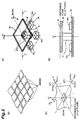
- the configuration of the spatial light modulation unit (first spatial light modulation unit) composed of the first and second spatial light modulators 2, 3 will be described below with reference to Fig. 2 .
- the area (a) of Fig. 2 is a perspective view showing the two-dimensional arrangement of mirror elements 2a in the first spatial light modulator 2 (or mirror elements 3a in the second spatial light modulator 3), the area (b) of Fig. 2 a drawing for explaining parameters for control on the postures of the mirror elements 2a (3a), the area (c) of Fig. 2 a partial perspective view showing one of the mirror elements 2a (3a), and the area (d) of Fig.
- FIG. 2 a drawing showing a cross section along line I-I, of the mirror element 2a (3a) shown in the area (c) of Fig. 2 . It is noted that the areas (a) to (d) of Fig. 2 are depicted without hatching for sections, for easier viewing.
- Each of the first and second spatial light modulators 2, 3, as shown in the area (a) of Fig. 2 is a movable multi-mirror including the mirror elements 2a (3a) being a large number of micro reflecting elements laid with their reflecting surface of a planar shape up.
- Each mirror element 2a (3a) is movable and inclination of the reflecting surface (mirror surface) thereof, i.e., an angle and direction of inclination of the reflecting surface, is independently controlled by the control unit CR (posture control of the reflecting surfaces).
- Each mirror element 2a (3a) can be continuously or discretely rotated by a desired angle of rotation around each of axes of rotation along two directions parallel to the reflecting surface thereof and orthogonal to each other.
- each mirror element 2a (3a) is so configured that the inclination thereof can be controlled in two dimensions along the reflecting surface thereof.
- a preferred control method is to control the angle of rotation in multiple stages (e.g.,..., -2.5°, -2.0°,..., 0°, +0.5°,..., +2.5°,).
- the above-described posture control of the reflecting surface for each mirror element 2a (3a) is implemented by adjusting an angle ⁇ between a normal to a reference plane in each of the first and second spatial light modulators 2 (3) (z1-axis) and a normal to the reflecting surface (z2-axis), as shown in the area (b) of Fig. 2 .
- the reference plane herein is a plane coincident with the reflecting surface before the posture control, which is an x1-y1 plane defined by an xl-axis and a y1-axis orthogonal to the normal z2 to the reflecting surface before the posture control.
- the angle ⁇ between the normal z1 (z1-axis) to the reference plane and the normal z2 to the reflecting surface is given by a rotation angle component ⁇ x1 around the xl-axis and a rotation angle component ⁇ y1 around the yl-axis, as specific posture control information.
- the rotation angle component ⁇ x1 is an angle between the normal z1 to the reference plane and the normal z2 to the reflecting surface when the normal z2 is projected onto the y1-z1 plane
- the rotation angle component ⁇ y1 is an angle between the normal z1 to the reference plane and the normal z2 to the reflecting surface when the normal z2 is projected onto the x1-z1 plane.
- the contour of the mirror elements 2a (3a) is square in this embodiment, but the contour is not limited to it. However, the contour is preferably a shape permitting arrangement without a gap (the closest packing) in terms of light utilization efficiency.
- the gap between adjacent mirror elements 2a (3a) is preferably set to a necessary minimum level.
- the area (c) of Fig. 2 is a drawing schematically showing a configuration of one mirror element out of the plurality of mirror elements 2a (3a) in the first and second spatial light modulators 2, 3 and, more specifically, a drawing schematically showing a drive unit for controlling the posture of the reflecting surface in the mirror element 2a (3 a).
- the area (d) of Fig. 2 is a drawing showing a cross section of the mirror element 2a (3a) along line I-I shown in the area (c) of Fig. 2 . In the areas (c) and (d) of Fig.
- the mirror element 2a (3a) has a base 30, a support 31 disposed on this base 30, a plate member 32 connected to the support 31 on the opposite side to the base 30, a reflecting surface 33 consisting of a reflecting film formed on this plate member 32, and four electrodes 34a-34d arranged so as to surround the support 31 on the base 30.
- the plate member 32 is inclinable around two axes (xl-axis and yl-axis) orthogonal to each other on a plane parallel to the base 30 with a fulcrum at a joint to the support 31. Then potentials are given to the electrodes 34a-34d arranged at respective positions on the base side corresponding to the four corners of the plate member 32, to generate an electrostatic force between each electrode 34a-34d and the plate member 32, thereby varying the gap between each electrode 34a-34d and the plate member 32 (drive unit). This causes the plate member 32 to be inclined on the fulcrum of the support 31 and, therefore, the reflecting surface 33 formed on the plate member 32 is inclined.
- the micro fly's eye lens 7 is, for example, an optical element consisting of a large number of micro lenses with a positive refracting power arranged vertically and horizontally and densely, and is made by forming the micro lens group in a plane-parallel plate by etching.
- the micro fly's eye lens different from a fly's eye lens consisting of lens elements isolated from each other, the large number of micro lenses (micro refracting faces) are integrally formed without being isolated from each other.
- the micro fly's eye lens is an optical integrator of the same wavefront division type as the fly's eye lens, in that the lens elements are arranged vertically and horizontally.
- a beam incident to the micro fly's eye lens 7 is two-dimensionally divided by the large number of micro lenses and a light source is formed on a rear focal plane of each micro lens to which the beam is incident.
- a substantial surface illuminant consisting of a large number of light sources (which will be referred to hereinafter as a "secondary light source”) is formed on the rear focal plane of the micro fly's eye lens 7. Beams from the secondary light source formed on the rear focal plane of the micro fly's eye lens 7 pass through a condenser optical system 8 to superposedly illuminate a mask blind 9. It is also possible to dispose an aperture stop behind or in front of the micro fly's eye lens 7, in order to limit the beams.
- an illumination field of a rectangular shape according to the shape and focal length of each micro lens forming the micro fly's eye lens 7 is formed on the mask blind 9 as an illumination field stop.
- Beams passing through a rectangular aperture (light transmitting portion) of the mask blind 9 are subjected to focusing action of an imaging optical system 10 and are deflected by a path bending mirror 10c disposed in an optical path between a front unit 10a and a rear unit 10b of the imaging optical system 10, to superposedly illuminate a mask (reticle) M on which a predetermined pattern is formed.
- the imaging optical system 10 forms an image of the rectangular aperture of the mask blind 9 on the mask M.
- a beam passing through the mask M travels through a projection optical system PL to form an image of the mask pattern on a wafer W as a photosensitive substrate.
- the pattern of the mask M is sequentially transferred into each of exposure areas on the wafer W, by performing batch exposure or scan exposure while two-dimensionally driving and controlling the wafer W in a plane perpendicular to the optical axis AX of the projection optical system PL.
- the spatial light modulators 2, 3 applied herein are those continuously changing each of orientations (reflection directions) of the mirror elements 2a, 3a arranged two-dimensionally, as described above.
- Such spatial light modulators can be selected, for example, from the spatial light modulators disclosed in Japanese Patent Application Laid-open (Translation of PCT Application) No. 10-503300 and European Patent Application Publication EP 779530 corresponding thereto, Japanese Patent Application Laid-open No. 2004-78136 and U.S. Pat. No. 6,900,915 corresponding thereto, Japanese Patent Application Laid-open (Translation of PCT Application) No. 2006-524349 and U.S. Pat. No. 7,095,546 corresponding thereto, and Japanese Patent Application Laid-open No. 2006-113437 .
- the orientations of the mirror elements 2a, 3a arranged two-dimensionally may be controlled discretely in multiple stages.
- the drive unit 2b to operate according to the posture control signal from the control unit CR changes each of the postures of the mirror elements 2a, whereby the reflecting surface of each mirror element 2a is set in a predetermined orientation.
- Light reflected at respective predetermined angles by the mirror elements 2a of the first spatial light modulator 2 is then incident to the second spatial light modulator 3.
- beams having traveled via the respective mirror elements 2a of the first spatial light modulator 2 are incident to the corresponding mirror elements 3a of the second spatial light modulator 3 arranged two-dimensionally in one-to-one correspondence.
- the drive unit 3b to operate according to the posture control signal from the control unit CR also changes each of the postures of the mirror elements 3a, whereby each mirror element 3a is set in a predetermined orientation.
- Light reflected at respective predetermined angles by the mirror elements 3a of the second spatial light modulator 3 forms an illumination field, for example, consisting of a light intensity distribution of an annular shape centered on the optical axis AX, on the entrance plane of the micro fly's eye lens 7, according to the combination of the mirror elements 2a and the mirror elements 3a, the postures of the respective mirror elements 2a, 3a, and so on.
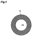
- the secondary light source with much the same light intensity distribution as the illumination field formed by the incident beam i.e., pupil intensity distribution 21 of an annular shape centered on the optical axis AX
- the secondary light source i.e., pupil intensity distribution 21 of an annular shape centered on the optical axis AX
- a light intensity distribution of an annular shape corresponding to the pupil intensity distribution 21 is also formed at other illumination pupil positions optically conjugate with the rear focal plane of the micro fly's eye lens 7, i.e., at the pupil position of the imaging optical system 10 and at the pupil position of the projection optical system PL.
- the condensing optical system 5 and the micro fly's eye lens 7 constitute a distribution forming optical system that forms a predetermined light intensity distribution on the illumination pupil, based on the beam having traveled via the first spatial light modulator 2 and the second spatial light modulator 3.
- the annular illumination field is formed on the entrance plane of the micro fly's eye lens 7 by the action of the pair of spatial light modulators 2, 3 and the annular light intensity distribution 21 is formed on the illumination pupil eventually, whereby annular illumination is implemented based on this annular pupil intensity distribution 21.
- multi-pole illumination dipole illumination, quadrupole illumination, or other illumination
- a multi-polar pupil intensity distribution for example, by forming a light intensity distribution of a multi-polar shape (dipolar shape, quadrupolar shape, or other shape) on the entrance plane of the micro fly's eye lens 7 and forming a light intensity distribution of a multi-polar shape on the illumination pupil eventually.
- the illumination optical apparatus (1 to 10) of the present embodiment has the spatial light modulation unit having the pair of spatial light modulators 2, 3, and the distribution forming optical system (5, 7) to form the light intensity distribution 21 on the illumination pupil on the basis of the beam having traveled via this spatial light modulation unit (2, 3).
- the orientations of the mirror elements 2a each are controlled so that beams having traveled via the respective mirror elements 2a of the first spatial light modulator 2 can be incident to the corresponding mirror elements 3a of the second spatial light modulator 3 arranged two-dimensionally in one-to-one correspondence to the mirror elements 2a, and the orientations of the mirror elements 3a of the second spatial light modulator 3 each are also controlled.
- the illumination optical apparatus (1 to 10) of this embodiment enables the simultaneous control on positions and angles of rays incident to the entrance plane of the micro fly's eye lens 7 by appropriately setting the combination of the mirror elements 2a of the first spatial light modulator 2 and the mirror elements 3a of the second spatial light modulator 3, the postures of the respective mirror elements 2a, 3a, and so on. Namely, it becomes feasible to simultaneously adjust (or correct) the shape and illuminance of the pupil intensity distribution 21 formed on the illumination pupil at the rear focal plane of the micro fly's eye lens 7, through the cooperation with the pair of spatial light modulators 2, 3.
- the pupil intensity distribution can be freely and quickly changed by the action of the pair of spatial light modulators 2, 3 in which the postures of the mirror elements 2a, 3a each are individually changed, and, therefore, the present embodiment is able to realize illumination conditions of great variety as to the shape and size of the pupil intensity distribution.
- the illumination optical apparatus (1 to 10) to illuminate the mask M as an illumination target surface on the basis of the light from the light source LS is able to form the pupil intensity distribution 21 of the desired shape and desired illuminance on the illumination pupil at the rear focal plane of the micro fly's eye lens 7 and, in turn, to realize the illumination conditions of great variety.
- the exposure apparatus (1 to PL) of the present embodiment is able to perform good exposure under an appropriate illumination condition realized according to a pattern characteristic of the mask M, using the illumination optical apparatus (1 to 10) capable of realizing the illumination conditions of great variety.
- the plane where the mirror elements are arranged makes the angle of about 45° with respect to the optical axis.
- the mirror elements near the optical axis are arranged at a desired position along the optical axis
- the mirror elements distant from the optical axis will positionally deviate in the optical-axis direction from the desired position.
- the positional deviation in the optical-axis direction of the mirror elements will cause an angle distribution of beams arriving at a point on the entrance plane of the fly's eye lens, to become rotationally asymmetric and thus it becomes difficult to keep the illuminance distribution constant on the wafer W.
- the pair of spatial light modulators 2, 3 are arranged so that the plane of the first spatial light modulator 2 where the mirror elements 2a are arranged and is opposed to the plane of the second spatial light modulator 3 where the mirror elements 3 a are arranged, e.g., so that these two planes become approximately parallel. Therefore, the influence of the positional deviation in the optical-axis direction of the mirror elements 2a, 3a distant from the optical axis AX is canceled out by the first spatial light modulator 2 and the second spatial light modulator 3, which facilitates achievement of keeping the illuminance distribution constant on the wafer W.
- the mirror elements 2a, 3a it is desirable to make a nearly parallel beam incident to the first spatial light modulator 2, i.e., to select a combination of the illumination optical apparatus with a light source which supplies a nearly parallel beam to the first spatial light modulator 2.
- the predetermined light intensity distribution is formed on the entrance plane of the micro fly's eye lens 7 being an optical integrator of the wavefront division type and, in turn, the predetermined pupil intensity distribution is realized.
- the predetermined pupil intensity distribution it is also feasible to realize the predetermined pupil intensity distribution, by forming a virtual image of the predetermined light intensity distribution on an entrance plane of an optical integrator of an internal reflection type.
- the above embodiment shows the configuration wherein the beams having traveled via the mirror elements 2a of the first spatial light modulator 2 are incident to the corresponding mirror elements 3a of the second spatial light modulator 3 arranged two-dimensionally in the one-to-one correspondence to the mirror elements 2a, but it is also possible to adopt a configuration wherein a beam having traveled via one of the mirror elements 2a of the first spatial light modulator 2 is incident to two or more mirror elements 3a of the second spatial light modulator 3.
- the mirror elements 2a of the first spatial light modulator 2 and the mirror elements 3a of the second spatial light modulator 3 may be in a one-to-two or more relation.
- the beams having traveled via the mirror elements 2a of the first spatial light modulator 2 are diverging beams.
- the mirror elements 2a of the first spatial light modulator 2 and the mirror elements 3a of the second spatial light modulator 3 are in a two or more-to-one relation.
- the mirror elements 2a of the first spatial light modulator 2 and the mirror elements 3a of the second spatial light modulator 3 may be in a two or more-to-two or more relation (e.g., like a case where two mirror elements 2a of the first spatial light modulator 2 correspond to three mirror elements 3a of the second spatial light modulator 3).
- the pair of spatial light modulators 2, 3 are arranged so that the plane where the mirror elements 2a of the first spatial light modulator 2 are arranged is approximately parallel to the plane where the mirror elements 3a of the second spatial light modulator 3 are arranged.
- various forms can be contemplated as to the arrangement of the pair of spatial light modulators 2, 3.
- a pair of spatial light modulators 2A, 3A may be three-dimensionally arranged so that the first spatial light modulator 2A reflects (or deflects) light incident in the x-direction, into the -z direction and so that the second spatial light modulator 3A reflects light incident in the -z direction, into the -y direction.
- a plane reflector 41 is additionally provided in the optical path between the first spatial light modulator 2B and the second spatial light modulator 3B.
- the pair of spatial light modulators 2B, 3B may be arranged in a V-shape so that light incident to the plane reflector 41 via the first spatial light modulator 2B is guided to the second spatial light modulator 3B.
- a second spatial light modulation unit may be incorporated in the sending optical system 1 to guide the beam from the light source LS to the spatial light modulation unit (2, 3).
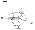
- the sending optical system 1A according to a modification example shown in Fig. 6 is provided with a shaping optical system 11 to convert the beam supplied from the light source LS, into a beam having a cross section of an appropriate size and shape. The beam through the shaping optical system 11 is then incident to a beam splitter 12.
- a beam reflected by the beam splitter 12 to the outside of the illumination optical path is incident to a detector 13.
- An output signal from the detector 13 is supplied to a control unit CR1.
- a beam transmitted by the beam splitter 12 and guided along the illumination optical path is successively incident to the first spatial light modulator 14 and the second spatial light modulator 15 in the second spatial light modulation unit.
- the beam having traveled via the second spatial light modulation unit (14, 15) is emitted from the sending optical system 1A to be guided to the first spatial light modulator 2 in the first spatial light modulation unit (2, 3).
- the second spatial light modulation unit (14, 15) has much the same configuration as the first spatial light modulation unit (2, 3). Namely, the first spatial light modulator 14 has a plurality of mirror elements 14a arranged two-dimensionally, and a drive unit 14b to individually change the postures of the mirror elements 14a in accordance with a posture control signal from the control unit CR1.
- the second spatial light modulator 15 has a plurality of mirror elements 15a arranged two-dimensionally, and a drive unit 15b to individually change the postures of the mirror elements 15a in accordance with a posture control signal from the control unit CR1.
- the mirror elements 15a of the second spatial light modulator 15 are two-dimensionally arranged in one-to-one correspondence to the mirror elements 14a of the first spatial light modulator 14, and the postures thereof are individually controlled.
- the drive unit 14b to operate according to the posture control signal from the control unit CR1 adjusts each of the postures of the mirror elements 14a, whereby each mirror element 14a is set in a predetermined orientation.
- Light reflected at respective predetermined angles by the mirror elements 14a of the first spatial light modulator 14 is incident to the second spatial light modulator 15.
- beams having traveled via the respective mirror elements 14a of the first spatial light modulator 14 are incident to the corresponding mirror elements 15a of the second spatial light modulator 15 which are two-dimensionally arranged in the one-to-one correspondence to the mirror elements 14a.
- the drive unit 15b to operate according to the posture control signal from the control unit CR1 also adjusts each of the postures of the mirror elements 15a, whereby each mirror element 15a is set in a predetermined orientation.
- Light reflected at respective predetermined angles by the mirror elements 15a of the second spatial light modulator 15 is converted into beams with a predetermined light intensity distribution according to the combination of the mirror elements 14a and the mirror elements 15a and the like and the beams are emitted from the sending optical system 1 A.
- the beam splitter 12 and detector 13 constitute a distribution measuring unit to measure the light intensity distribution of the beam incident from the light source LS to the second spatial light modulation unit (14, 15).
- the control unit CR1 constitutes a control unit to control the second spatial light modulation unit (14, 15) on the basis of the result of the measurement by the distribution measuring unit (12, 13).
- the distribution measuring unit (12, 13) measures the light intensity distribution of the beam incident to the second spatial light modulation unit (14, 15) and the control unit CR1 individually controls the postures of the respective mirror elements 14a, 15a in the second spatial light modulation unit (14, 15) on the basis of the measurement result by the distribution measuring unit (12, 13).
- This configuration makes it feasible to appropriately convert the incident beam into the beam with the desired light intensity distribution and emit the converted beam.
- a beam supplied from an ArF excimer laser light source or a KrF excimer laser light source has a light intensity distribution of a form wherein the light intensity is higher in the center than in the periphery.
- an optical material of each optical member arranged in the illumination optical path is more likely to deteriorate, particularly, in its central region where the energy density of the incident beam is high.
- a phenomenon of "clouding" on an optical surface is likely to occur because of adhesion of a material to the optical surface, damage of the optical surface due to photochemical reaction, and so on.
- the sending optical system 1A is able to convert the incident light into a beam with a desired light intensity distribution, e.g., a nearly even light intensity distribution, and to guide the converted beam to the first spatial light modulation unit (2, 3). Therefore, it is feasible to well suppress the damage, deterioration of optical properties, etc. of the optical members arranged behind the sending optical system 1A, particularly, each mirror element 2a, 3a in the first spatial light modulation unit (2, 3) arranged immediately after the sending optical system 1A.
- the second spatial light modulation unit (14, 15) in the sending optical system 1A there is no optical member arranged in the optical path between the first spatial light modulator 14 and the second spatial light modulator 15, but, without having to be limited to this, a relay optical system or the like may be arranged in this optical path.
- a relay optical system or the like may be arranged in this optical path.
- the pair of spatial light modulators 14, 15 are arranged so that the plane of the first spatial light modulator 14 where the mirror elements 14a are arranged is approximately parallel to the plane of the second spatial light modulator 15 where the mirror elements 15a are arranged.
- various forms can also be contemplated as to the arrangement of the pair of spatial light modulators 14, 15, as in the case of the first spatial light modulation unit (2, 3).
- the spatial light modulators in which the orientations (angles: inclinations) of the reflecting surfaces arranged two-dimensionally can be individually controlled are applied as the spatial light modulators with the plurality of optical elements arranged two-dimensionally and posture-controlled individually.
- Such spatial light modulators applicable herein can be selected, for example, from those disclosed in Japanese Patent Application Laid-open No. 6-281869 and U.S. Pat. No. 5,312,513 corresponding thereto, and in Fig. Id of Japanese Patent Application Laid-open (Translation of PCT Application) No.
- spatial light modulators are able to apply the same action as a diffracting surface, to incident light by forming a two-dimensional height distribution therein.
- the aforementioned spatial light modulators with the plurality of reflecting surfaces arranged two-dimensionally may be modified, for example, according to the disclosure in Japanese Patent Application Laid-open (Translation of PCT Application) No. 2006-513442 and U.S. Pat. No. 6,891,655 corresponding thereto, or according to the disclosure in Japanese Patent Application Laid-open (Translation of PCT Application) No. 2005-524112 and U.S. Pat. Published Application No. 2005/0095749 corresponding thereto.
- each spatial light modulator applied is the reflective spatial light modulator with the plurality of mirror elements, but, without having to be limited to this, it is also possible, for example, to apply the transmissive spatial light modulator disclosed in
- the optical system may be modified so that in the formation of the pupil intensity distribution using the spatial light modulators, the pupil intensity distribution is measured with a pupil intensity distribution measuring device and the spatial light modulators are controlled according to the result of the measurement.
- Such technology is disclosed, for example, in Japanese Patent Application Laid-open No. 2006-54328 and in Japanese Patent Application Laid-open No. 2003-22967 and U.S. Pat. Published Application No. 2003/0038225 corresponding thereto.
- the mask can be replaced with a variable pattern forming device which forms a predetermined pattern on the basis of predetermined electronic data.
- a variable pattern forming device can be, for example, a DMD (Digital Micromirror Device) including a plurality of reflective elements driven based on predetermined electronic data.
- the exposure apparatus with the DMD is disclosed, for example, in Japanese Patent Application Laid-open No. 2004-304135 and International Publication WO2006/080285 and U.S Pat. Published Application No. 2007/0296936 corresponding thereto.
- variable pattern forming device can also be applied in cases where the pattern surface is set horizontal.
- the exposure apparatus of the foregoing embodiment is manufactured by assembling various sub-systems containing their respective components as set forth in the scope of claims in the present application, so as to maintain predetermined mechanical accuracy, electrical accuracy, and optical accuracy.
- the following adjustments are carried out before and after the assembling: adjustment for achieving the optical accuracy for various optical systems; adjustment for achieving the mechanical accuracy for various mechanical systems; adjustment for achieving the electrical accuracy for various electrical systems.
- the assembling steps from the various sub-systems into the exposure apparatus include mechanical connections, wire connections of electric circuits, pipe connections of pneumatic circuits, etc. between the various sub-systems.
- Fig. 7 is a flowchart for explaining manufacturing steps of semiconductor devices, as an embodiment of the device manufacturing method according to the present invention.
- the manufacturing steps of semiconductor devices include depositing a metal film on a wafer W to become a substrate of semiconductor devices (step S40) and applying a photoresist as a photosensitive material onto the deposited metal film (step S42).
- the subsequent steps include transferring a pattern formed on a mask (reticle) M, into each shot area on the wafer W, using the aforementioned projection exposure apparatus (step S44: exposure step), and developing the wafer W after completion of the transfer, i.e., developing the photoresist to which the pattern has been transferred (step S46: development step). Thereafter, using the resist pattern made on the surface of the wafer W in step S46, as a mask, processing such as etching is carried out on the surface of the wafer W (step S48: processing step).
- the resist pattern herein is a photoresist layer in which depressions and projections are formed in a shape corresponding to the pattern transferred by the projection exposure apparatus and which the depressions penetrate throughout.
- Step S48 is to process the surface of the wafer W through this resist pattern.
- the processing carried out in step S48 includes, for example, at least either etching of the surface of the wafer W or deposition of a metal film or the like.
- the projection exposure apparatus performs the transfer of the pattern onto the wafer W coated with the photoresist, as a photosensitive substrate or plate P.
- Fig. 8 is a flowchart for explaining manufacturing steps of a liquid crystal device such as a liquid-crystal display device, as another embodiment of the device manufacturing method according to the present invention.
- the manufacturing steps of the liquid crystal device include sequentially performing a pattern forming step (step S50), a color filter forming step (step S52), a cell assembly step (step S54), and a module assembly step (step S56).
- the pattern forming step of step S50 is to form predetermined patterns such as a circuit pattern and an electrode pattern on a glass substrate coated with a photoresist, as a plate P, using the aforementioned projection exposure apparatus.
- This pattern forming step includes an exposure step of transferring a pattern to a photoresist layer, using the projection exposure apparatus, a development step of performing development of the plate P to which the pattern has been transferred, i.e., development of the photoresist layer on the glass substrate, and making the photoresist layer in the shape corresponding to the pattern, and a processing step of processing the surface of the glass substrate through the developed photoresist layer.
- the color filter forming step of step S52 is to form a color filter in which a large number of sets of three dots corresponding to R (Red), G (Green), and B (Blue) are arrayed in a matrix pattern, or in which a plurality of filter sets of three stripes of R, G, and B are arrayed in a horizontal scan direction.
- the cell assembly step of step S54 is to assemble a liquid crystal panel (liquid crystal cell), using the glass substrate on which the predetermined pattern has been formed in step S50, and the color filter formed in step S52. Specifically, a liquid crystal is poured into between the glass substrate and the color filter to form the liquid crystal panel.
- the module assembly step of step S56 is to attach various components such as electric circuits and backlights for display operation of this liquid crystal panel, to the liquid crystal panel assembled in step S54.
- the present invention is not limited just to the application to the exposure apparatus for manufacture of semiconductor devices, but can also be widely applied, for example, to the exposure apparatus for the liquid-crystal display devices formed with rectangular glass plates, or for display devices such as plasma displays, and the exposure apparatus for manufacture of various devices such as imaging devices (CCDs and others), micromachines, thin-film magnetic heads, and DNA chips. Furthermore, the present invention is also applicable to the exposure step (exposure apparatus) for manufacture of masks (photomasks, reticles, etc.) on which mask patterns of various devices are formed, by the photolithography process.
- the present invention can also be applied to any other appropriate laser light source, e.g., an F 2 laser light source which supplies laser light at the wavelength of 157 nm.
- a technique of filling the interior of the optical path between the projection optical system and the photosensitive substrate with a medium having the refractive index larger than 1.1 typically, a liquid
- a liquid immersion method it is possible to adopt one of the following techniques as a technique of filing the interior of the optical path between the projection optical system and the photosensitive substrate with the liquid: the technique of locally filling the optical path with the liquid as disclosed in International Publication WO99/49504 ; the technique of moving a stage holding the substrate to be exposed, in a liquid bath as disclosed in Japanese Patent Application Laid-open No. 6-124873 ; the technique of forming a liquid bath of a predetermined depth on a stage and holding the substrate therein as disclosed in Japanese Patent Application Laid-open No. 10-303114 , and so on.
- the aforementioned embodiment was the application of the present invention to the illumination optical apparatus illuminating the mask in the exposure apparatus, but, without having to be limited to this, the present invention can also be applied to a generally-used illumination optical apparatus which illuminates an illumination target surface except for the mask.
Abstract
Description
- The present invention relates to a spatial light modulation unit, an illumination optical apparatus, an exposure apparatus, and a device manufacturing method. More particularly, the present invention relates to an illumination optical apparatus suitably applicable to an exposure apparatus for manufacturing such devices as semiconductor devices, imaging devices, liquid-crystal display devices, and thin-film magnetic heads by lithography.
- In a typical exposure apparatus of this type, a light beam emitted from a light source travels through a fly's eye lens as an optical integrator to form a secondary light source (a predetermined light intensity distribution on an illumination pupil in general) as a substantial surface illuminant consisting of a large number of light sources. In this specification the light intensity distribution on the illumination pupil will be referred to hereinafter as a "pupil intensity distribution." The illumination pupil is defined as a position such that an illumination target surface becomes a Fourier transform surface of the illumination pupil by action of an optical system between the illumination pupil and the illumination target surface (a mask or a wafer in the case of the exposure apparatus).
- Beams from the secondary light source are condensed by a condenser lens to superposedly illuminate the mask on which a predetermined pattern is formed. Light passing through the mask travels through a projection optical system to be focused on the wafer, whereby the mask pattern is projected (or transferred) onto the wafer to effect exposure thereof. Since the pattern formed on the mask is a highly integrated one, an even illuminance distribution must be obtained on the wafer in order to accurately transfer this fine pattern onto the wafer.
- There is a hitherto proposed illumination optical apparatus capable of continuously changing the pupil intensity distribution (and, in turn, an illumination condition) without use of a zoom optical system (see Patent Document 1). The illumination optical apparatus disclosed in
Patent Document 1 is configured using a movable multi-mirror composed of a large number of micro mirror elements which are arranged in an array form and an inclination angle and inclination direction of each of which are individually driven and controlled. An incident beam is deflected in a state in which the beam is divided in micro units by respective reflecting surfaces in the movable multi-mirror. The movable multi-mirror converts a cross section of the incident beam into a desired shape and size and, in turn, realizes a desired pupil intensity distribution.
Patent Document 1: Japanese Patent Application Laid-open No.2002-353105 - The present inventors have examined the above prior art, and as a result, have discovered the following problems.
- Namely, since the illumination optical apparatus described in
Patent Document 1 uses the movable multi-mirror singly as a spatial light modulator, it is unable to simultaneously control positions and angles of rays incident to the entrance plane of the fly's eye lens. As a consequence, when the pupil intensity distribution is attempted to be set in a desired shape, it becomes difficult to achieve constant illuminance; conversely, when the illuminance is attempted to be set at a constant level in the pupil intensity distribution, it becomes difficult to obtain the pupil intensity distribution in a desired shape. - The present invention has been accomplished in order to solve the problem as described above, and an object of the invention is to provide an illumination optical apparatus capable of forming a pupil intensity distribution of a desired shape and desired illuminance and therefore capable of realizing illumination conditions of great variety, a spatial light modulation unit applicable to the illumination optical apparatus, an exposure apparatus capable of performing good exposure under an appropriate illumination condition realized according to a pattern characteristic, using the illumination optical apparatus capable of realizing the illumination conditions of great variety, and a device manufacturing method using the exposure apparatus.
- In order to solve the above-described problem, a spatial light modulation unit according to the present invention is arranged in an optical path of an illumination optical apparatus and comprises a first spatial light modulator and a second spatial light modulator arranged in an order of incidence of light. The first spatial light modulator has a plurality of first optical elements which are two-dimensionally arranged and postures of which each are individually controlled. The second spatial light modulator has a plurality of second optical elements which are two-dimensionally arranged in correspondence to the plurality of first optical elements and postures of which each are individually controlled.
- An illumination optical apparatus according to the present invention illuminates an illumination target surface on the basis of light from a light source. The illumination optical apparatus comprises a spatial light modulation unit having the structure as described above (the spatial light modulation unit according to the present invention), and a distribution forming optical system to form a predetermined light intensity distribution on an illumination pupil of the illumination optical apparatus, based on a beam having traveled via the first spatial light modulator and the second spatial light modulator.
- An exposure apparatus according to the present invention comprises an illumination optical apparatus having the structure as described above (the illumination optical apparatus according to the present invention), and the exposure apparatus performing exposure of a predetermined pattern illuminated by the illumination optical apparatus, on a photosensitive substrate.
- A device manufacturing method according to the present invention comprises an exposure step, a development step, and a processing step. The exposure step is to effect exposure of a predetermined pattern on a photosensitive substrate, using an exposure apparatus having the structure as described above (the exposure apparatus according to the present invention). The development step is to develop the photosensitive substrate onto which the predetermined pattern has been transferred, and then form a mask layer in a shape corresponding to the predetermined pattern on a surface of the photosensitive substrate. The processing step is to process the surface of the photosensitive substrate through the mask layer.
- The present invention will be more fully understood from the detailed description given hereinbelow and the accompanying drawings, which are given by way of illustration only and are not to be considered as limiting the present invention.
- Further scope of applicability of the present invention will become apparent from the detailed description given hereinafter. However, it should be understood that the detailed description and specific examples, while indicating preferred embodiments of the invention, are given by way of illustration only, since various changes and modifications within the scope of the invention will be apparent to those skilled in the art from this detailed description.
- In the illumination optical apparatus according to the present invention, the light having traveled sequentially via the pair of spatial light modulators travels via the condensing optical system functioning, for example, as a Fourier transform lens to enter the optical integrator. As a result, the cooperation of the pair of spatial light modulators enables the simultaneous control of positions and angles of rays incident to the entrance plane of the optical integrator and, in turn, enables simultaneous adjustment (or correction) for the shape and illuminance of the pupil intensity distribution.
- In this manner, the illumination optical apparatus according to the present invention is able to form the pupil intensity distribution of the desired shape and desired illuminance and, in turn, to realize the illumination conditions of great variety. The exposure apparatus according to the present invention is able to perform good exposure under an appropriate illumination condition realized according to a pattern characteristic of a mask, using the foregoing illumination optical apparatus capable of realizing the illumination conditions of great variety, and, in turn, to manufacture good devices.
-
-
Fig. 1 is a drawing schematically showing a configuration of an exposure apparatus according to the present invention (incorporating the spatial light modulation unit and the illumination optical apparatus according to the present invention); -
Fig. 2 shows drawings for schematically explaining a configuration of each of spatial light modulators in the exposure apparatus shown inFig. 1 ; -
Fig. 3 is a drawing schematically showing an annular pupil intensity distribution formed on a rear focal plane of a micro fly's eye lens; -
Fig. 4 is a drawing schematically showing another arrangement example of a pair of spatial light modulators; -
Fig. 5 is a drawing schematically showing still another arrangement example of a pair of spatial light modulators; -
Fig. 6 is a drawing schematically showing an internal configuration of a sending optical system in which a second spatial light modulation unit is incorporated; -
Fig. 7 is a flowchart for explaining manufacturing steps of semiconductor devices, as an embodiment of the device manufacturing method according to the present invention; and -
Fig. 8 is a flowchart for explaining manufacturing steps of a liquid crystal device such as a liquid crystal display device, as another embodiment of the device manufacturing method according to the present invention. - 1···sending optical system; 2, 3···spatial light modulator, 2a, 3a ···plural mirror elements in spatial light modulator; 5···condensing optical system (Fourier transform lens); 7···micro fly's eye lens; 8··· condenser optical system; 9···mask blind; 10···imaging optical system; Ls···light source; CR···control unit; M···mask; PL···projection optical system; and W···wafer.
- Embodiments of the spatial light modulation unit, illumination optical apparatus, exposure apparatus, and device manufacturing method according to the present invention will be described below in detail with reference to
Figs. 1 to 8 . In the description of the drawings, the same portions and the same elements will be denoted by the same reference symbols, without redundant description. -
Fig. 1 is a drawing schematically showing a configuration of the exposure apparatus according to the present invention. InFig. 1 , the Z-axis is set along a direction of a normal to a wafer W being a photosensitive substrate, the Y-axis along a direction parallel to the plane ofFig. 1 in a plane of the wafer W, and the X-axis along a direction normal to the plane ofFig. 1 in the plane of the wafer W. - Referring to
Fig. 1 , a light source LS supplies exposure light (illumination light) to the exposure apparatus according to the present embodiment. The light source LS applicable herein is, for example, an ArF excimer laser light source which supplies light at the wavelength of 193 nm, or a KrF excimer laser light source which supplies light at the wavelength of 248 nm. A light beam emitted along the optical axis and in the Z-direction from the light source LS travels through a sendingoptical system 1 having a well-known configuration and is sequentially incident to a first spatiallight modulator 2 and a second spatiallight modulator 3. - The sending
optical system 1 has functions to convert the incident beam into a beam with a cross section of an appropriate size and shape and guide the thus-shaped beam to the first spatiallight modulator 2, and to actively correct positional variation and angular variation of the beam incident to the first spatiallight modulator 2. The first spatiallight modulator 2 has a plurality of mirror elements (optical elements in general) 2a arranged two-dimensionally, and adrive unit 2b which individually controls and drives postures of themirror elements 2a in accordance with a posture control signal from a control unit CR. - The second spatial
light modulator 3 also has a plurality ofmirror elements 3a (optical elements in general) arranged two-dimensionally, and adrive unit 3b which individually controls and drives postures of themirror elements 34a in accordance with a posture control signal from the control unit CR as the first spatiallight modulator 2 does. Themirror elements 3a of the second spatiallight modulator 3 are two-dimensionally arranged in one-to-one correspondence to themirror elements 2a of the first spatiallight modulation unit 2, and the postures thereof are individually controlled. The action of the spatial light modulation unit having the first spatiallight modulator 2 and the second spatiallight modulator 3 will be described hereinbelow. - The configuration of the spatial light modulation unit (first spatial light modulation unit) composed of the first and second spatial
light modulators Fig. 2 . The area (a) ofFig. 2 is a perspective view showing the two-dimensional arrangement ofmirror elements 2a in the first spatial light modulator 2 (ormirror elements 3a in the second spatial light modulator 3), the area (b) ofFig. 2 a drawing for explaining parameters for control on the postures of themirror elements 2a (3a), the area (c) ofFig. 2 a partial perspective view showing one of themirror elements 2a (3a), and the area (d) ofFig. 2 a drawing showing a cross section along line I-I, of themirror element 2a (3a) shown in the area (c) ofFig. 2 . It is noted that the areas (a) to (d) ofFig. 2 are depicted without hatching for sections, for easier viewing. - Each of the first and second spatial
light modulators Fig. 2 , is a movable multi-mirror including themirror elements 2a (3a) being a large number of micro reflecting elements laid with their reflecting surface of a planar shape up. Eachmirror element 2a (3a) is movable and inclination of the reflecting surface (mirror surface) thereof, i.e., an angle and direction of inclination of the reflecting surface, is independently controlled by the control unit CR (posture control of the reflecting surfaces). Eachmirror element 2a (3a) can be continuously or discretely rotated by a desired angle of rotation around each of axes of rotation along two directions parallel to the reflecting surface thereof and orthogonal to each other. Namely, eachmirror element 2a (3a) is so configured that the inclination thereof can be controlled in two dimensions along the reflecting surface thereof. In the case of discrete rotation, a preferred control method is to control the angle of rotation in multiple stages (e.g.,..., -2.5°, -2.0°,..., 0°, +0.5°,..., +2.5°,...). - The above-described posture control of the reflecting surface for each
mirror element 2a (3a) is implemented by adjusting an angle θ between a normal to a reference plane in each of the first and second spatial light modulators 2 (3) (z1-axis) and a normal to the reflecting surface (z2-axis), as shown in the area (b) ofFig. 2 . The reference plane herein is a plane coincident with the reflecting surface before the posture control, which is an x1-y1 plane defined by an xl-axis and a y1-axis orthogonal to the normal z2 to the reflecting surface before the posture control. The angle θ between the normal z1 (z1-axis) to the reference plane and the normal z2 to the reflecting surface is given by a rotation angle component θx1 around the xl-axis and a rotation angle component θy1 around the yl-axis, as specific posture control information. Specifically, the rotation angle component θx1 is an angle between the normal z1 to the reference plane and the normal z2 to the reflecting surface when the normal z2 is projected onto the y1-z1 plane, and the rotation angle component θy1 is an angle between the normal z1 to the reference plane and the normal z2 to the reflecting surface when the normal z2 is projected onto the x1-z1 plane. - In addition, the contour of the
mirror elements 2a (3a) is square in this embodiment, but the contour is not limited to it. However, the contour is preferably a shape permitting arrangement without a gap (the closest packing) in terms of light utilization efficiency. The gap betweenadjacent mirror elements 2a (3a) is preferably set to a necessary minimum level. - The area (c) of
Fig. 2 is a drawing schematically showing a configuration of one mirror element out of the plurality ofmirror elements 2a (3a) in the first and second spatiallight modulators mirror element 2a (3 a). The area (d) ofFig. 2 is a drawing showing a cross section of themirror element 2a (3a) along line I-I shown in the area (c) ofFig. 2 . In the areas (c) and (d) ofFig. 2 , themirror element 2a (3a) has abase 30, asupport 31 disposed on thisbase 30, aplate member 32 connected to thesupport 31 on the opposite side to thebase 30, a reflectingsurface 33 consisting of a reflecting film formed on thisplate member 32, and fourelectrodes 34a-34d arranged so as to surround thesupport 31 on thebase 30. - The
plate member 32 is inclinable around two axes (xl-axis and yl-axis) orthogonal to each other on a plane parallel to the base 30 with a fulcrum at a joint to thesupport 31. Then potentials are given to theelectrodes 34a-34d arranged at respective positions on the base side corresponding to the four corners of theplate member 32, to generate an electrostatic force between eachelectrode 34a-34d and theplate member 32, thereby varying the gap between eachelectrode 34a-34d and the plate member 32 (drive unit). This causes theplate member 32 to be inclined on the fulcrum of thesupport 31 and, therefore, the reflectingsurface 33 formed on theplate member 32 is inclined. - Light successively reflected by the
mirror elements 2a of the first spatiallight modulator 2 and by themirror elements 3a of the second spatiallight modulator 3 travels via a fixed stop (flare stop) 4, a condensingoptical system 5 as a Fourier transform lens, and apath bending mirror 6 to enter a micro fly's eye lens (or fly's eye lens) 7 as an optical integrator. The micro fly's eye lens 7 is, for example, an optical element consisting of a large number of micro lenses with a positive refracting power arranged vertically and horizontally and densely, and is made by forming the micro lens group in a plane-parallel plate by etching. - In the micro fly's eye lens, different from a fly's eye lens consisting of lens elements isolated from each other, the large number of micro lenses (micro refracting faces) are integrally formed without being isolated from each other. However, the micro fly's eye lens is an optical integrator of the same wavefront division type as the fly's eye lens, in that the lens elements are arranged vertically and horizontally. A beam incident to the micro fly's eye lens 7 is two-dimensionally divided by the large number of micro lenses and a light source is formed on a rear focal plane of each micro lens to which the beam is incident.
- Namely, a substantial surface illuminant consisting of a large number of light sources (which will be referred to hereinafter as a "secondary light source") is formed on the rear focal plane of the micro fly's eye lens 7. Beams from the secondary light source formed on the rear focal plane of the micro fly's eye lens 7 pass through a condenser
optical system 8 to superposedly illuminate amask blind 9. It is also possible to dispose an aperture stop behind or in front of the micro fly's eye lens 7, in order to limit the beams. - In this manner, an illumination field of a rectangular shape according to the shape and focal length of each micro lens forming the micro fly's eye lens 7 is formed on the
mask blind 9 as an illumination field stop. Beams passing through a rectangular aperture (light transmitting portion) of themask blind 9 are subjected to focusing action of an imagingoptical system 10 and are deflected by apath bending mirror 10c disposed in an optical path between afront unit 10a and arear unit 10b of the imagingoptical system 10, to superposedly illuminate a mask (reticle) M on which a predetermined pattern is formed. - Namely, the imaging
optical system 10 forms an image of the rectangular aperture of themask blind 9 on the mask M. A beam passing through the mask M travels through a projection optical system PL to form an image of the mask pattern on a wafer W as a photosensitive substrate. In this way, the pattern of the mask M is sequentially transferred into each of exposure areas on the wafer W, by performing batch exposure or scan exposure while two-dimensionally driving and controlling the wafer W in a plane perpendicular to the optical axis AX of the projection optical system PL. - In the present embodiment, the spatial
light modulators mirror elements 10-503300 EP 779530 2004-78136 U.S. Pat. No. 6,900,915 corresponding thereto, Japanese Patent Application Laid-open (Translation of PCT Application) No.2006-524349 U.S. Pat. No. 7,095,546 corresponding thereto, and Japanese Patent Application Laid-open No.2006-113437 mirror elements - In the first spatial
light modulator 2, thedrive unit 2b to operate according to the posture control signal from the control unit CR changes each of the postures of themirror elements 2a, whereby the reflecting surface of eachmirror element 2a is set in a predetermined orientation. Light reflected at respective predetermined angles by themirror elements 2a of the first spatiallight modulator 2 is then incident to the second spatiallight modulator 3. Specifically, beams having traveled via therespective mirror elements 2a of the first spatiallight modulator 2 are incident to thecorresponding mirror elements 3a of the second spatiallight modulator 3 arranged two-dimensionally in one-to-one correspondence. - In the second spatial
light modulator 3, similar to the first spatiallight modulator 2, thedrive unit 3b to operate according to the posture control signal from the control unit CR also changes each of the postures of themirror elements 3a, whereby eachmirror element 3a is set in a predetermined orientation. Light reflected at respective predetermined angles by themirror elements 3a of the second spatiallight modulator 3 forms an illumination field, for example, consisting of a light intensity distribution of an annular shape centered on the optical axis AX, on the entrance plane of the micro fly's eye lens 7, according to the combination of themirror elements 2a and themirror elements 3a, the postures of therespective mirror elements - In this manner, as shown in
Fig. 3 , the secondary light source with much the same light intensity distribution as the illumination field formed by the incident beam, i.e.,pupil intensity distribution 21 of an annular shape centered on the optical axis AX, is formed on the rear focal plane of the micro fly's eye lens 7 (and, therefore, on the illumination pupil). Furthermore, a light intensity distribution of an annular shape corresponding to thepupil intensity distribution 21 is also formed at other illumination pupil positions optically conjugate with the rear focal plane of the micro fly's eye lens 7, i.e., at the pupil position of the imagingoptical system 10 and at the pupil position of the projection optical system PL. As described above, the condensingoptical system 5 and the micro fly's eye lens 7 constitute a distribution forming optical system that forms a predetermined light intensity distribution on the illumination pupil, based on the beam having traveled via the first spatiallight modulator 2 and the second spatiallight modulator 3. - In the above description, the annular illumination field is formed on the entrance plane of the micro fly's eye lens 7 by the action of the pair of spatial
light modulators light intensity distribution 21 is formed on the illumination pupil eventually, whereby annular illumination is implemented based on this annularpupil intensity distribution 21. However, without having to be limited to the annular illumination, it is also possible to implement multi-pole illumination (dipole illumination, quadrupole illumination, or other illumination) based on a multi-polar pupil intensity distribution, for example, by forming a light intensity distribution of a multi-polar shape (dipolar shape, quadrupolar shape, or other shape) on the entrance plane of the micro fly's eye lens 7 and forming a light intensity distribution of a multi-polar shape on the illumination pupil eventually. - The illumination optical apparatus (1 to 10) of the present embodiment has the spatial light modulation unit having the pair of spatial
light modulators light intensity distribution 21 on the illumination pupil on the basis of the beam having traveled via this spatial light modulation unit (2, 3). In the spatial light modulation unit (2, 3), the orientations of themirror elements 2a each are controlled so that beams having traveled via therespective mirror elements 2a of the first spatiallight modulator 2 can be incident to thecorresponding mirror elements 3a of the second spatiallight modulator 3 arranged two-dimensionally in one-to-one correspondence to themirror elements 2a, and the orientations of themirror elements 3a of the second spatiallight modulator 3 each are also controlled. - In this manner, the illumination optical apparatus (1 to 10) of this embodiment enables the simultaneous control on positions and angles of rays incident to the entrance plane of the micro fly's eye lens 7 by appropriately setting the combination of the
mirror elements 2a of the first spatiallight modulator 2 and themirror elements 3a of the second spatiallight modulator 3, the postures of therespective mirror elements pupil intensity distribution 21 formed on the illumination pupil at the rear focal plane of the micro fly's eye lens 7, through the cooperation with the pair of spatiallight modulators - It is important for the exposure apparatus to perform exposure under an appropriate illumination condition according to a pattern characteristic, in order to highly accurately and faithfully transfer the pattern of the mask M onto the wafer W. In this embodiment, the pupil intensity distribution can be freely and quickly changed by the action of the pair of spatial
light modulators mirror elements - As in the above-described embodiment, the illumination optical apparatus (1 to 10) to illuminate the mask M as an illumination target surface on the basis of the light from the light source LS is able to form the
pupil intensity distribution 21 of the desired shape and desired illuminance on the illumination pupil at the rear focal plane of the micro fly's eye lens 7 and, in turn, to realize the illumination conditions of great variety. The exposure apparatus (1 to PL) of the present embodiment is able to perform good exposure under an appropriate illumination condition realized according to a pattern characteristic of the mask M, using the illumination optical apparatus (1 to 10) capable of realizing the illumination conditions of great variety. - Since the illumination optical apparatus described in the
aforementioned Document 1 uses the movable multi-mirror singly as a spatial light modulator, the plane where the mirror elements are arranged makes the angle of about 45° with respect to the optical axis. In this case, when the mirror elements near the optical axis are arranged at a desired position along the optical axis, the mirror elements distant from the optical axis will positionally deviate in the optical-axis direction from the desired position. As a result, the positional deviation in the optical-axis direction of the mirror elements will cause an angle distribution of beams arriving at a point on the entrance plane of the fly's eye lens, to become rotationally asymmetric and thus it becomes difficult to keep the illuminance distribution constant on the wafer W. - In the present embodiment, the pair of spatial
light modulators light modulator 2 where themirror elements 2a are arranged and is opposed to the plane of the second spatiallight modulator 3 where themirror elements 3 a are arranged, e.g., so that these two planes become approximately parallel. Therefore, the influence of the positional deviation in the optical-axis direction of themirror elements light modulator 2 and the second spatiallight modulator 3, which facilitates achievement of keeping the illuminance distribution constant on the wafer W. - In the above embodiment there is no optical member arranged in the optical path between the first spatial
light modulator 2 and the second spatiallight modulator 3, but, without having to be limited to this, it is also possible to place a relay optical system or the like in this optical path. It is, however, desirable to place no optical member in the optical path or to place no optical member having a power in the optical path, in order to facilitate the setting of the one-to-one correspondence relation between themirror elements 2a of the first spatiallight modulator 2 and themirror elements 3a of the second spatiallight modulator 3. Furthermore, in order to facilitate the setting of the one-to-one correspondence relation between themirror elements light modulator 2, i.e., to select a combination of the illumination optical apparatus with a light source which supplies a nearly parallel beam to the first spatiallight modulator 2. - In the above embodiment, the predetermined light intensity distribution is formed on the entrance plane of the micro fly's eye lens 7 being an optical integrator of the wavefront division type and, in turn, the predetermined pupil intensity distribution is realized. However, without having to be limited to this, it is also feasible to realize the predetermined pupil intensity distribution, by forming a virtual image of the predetermined light intensity distribution on an entrance plane of an optical integrator of an internal reflection type.
- The above embodiment shows the configuration wherein the beams having traveled via the
mirror elements 2a of the first spatiallight modulator 2 are incident to thecorresponding mirror elements 3a of the second spatiallight modulator 3 arranged two-dimensionally in the one-to-one correspondence to themirror elements 2a, but it is also possible to adopt a configuration wherein a beam having traveled via one of themirror elements 2a of the first spatiallight modulator 2 is incident to two ormore mirror elements 3a of the second spatiallight modulator 3. In other words, themirror elements 2a of the first spatiallight modulator 2 and themirror elements 3a of the second spatiallight modulator 3 may be in a one-to-two or more relation. In this case, the beams having traveled via themirror elements 2a of the first spatiallight modulator 2 are diverging beams. - Conversely, it is also possible to adopt a configuration wherein the
mirror elements 2a of the first spatiallight modulator 2 and themirror elements 3a of the second spatiallight modulator 3 are in a two or more-to-one relation. Furthermore, themirror elements 2a of the first spatiallight modulator 2 and themirror elements 3a of the second spatiallight modulator 3 may be in a two or more-to-two or more relation (e.g., like a case where twomirror elements 2a of the first spatiallight modulator 2 correspond to threemirror elements 3a of the second spatial light modulator 3). - In the above embodiment, the pair of spatial
light modulators mirror elements 2a of the first spatiallight modulator 2 are arranged is approximately parallel to the plane where themirror elements 3a of the second spatiallight modulator 3 are arranged. However, without having to be limited to this, various forms can be contemplated as to the arrangement of the pair of spatiallight modulators - For example, as shown in
Fig. 4 , a pair of spatiallight modulators light modulator 2A reflects (or deflects) light incident in the x-direction, into the -z direction and so that the second spatiallight modulator 3A reflects light incident in the -z direction, into the -y direction. Furthermore, as shown inFig. 5 , it is also possible to adopt a configuration wherein aplane reflector 41 is additionally provided in the optical path between the first spatiallight modulator 2B and the second spatiallight modulator 3B. Namely, the pair of spatiallight modulators plane reflector 41 via the first spatiallight modulator 2B is guided to the second spatiallight modulator 3B. - In the above embodiment, a second spatial light modulation unit may be incorporated in the sending
optical system 1 to guide the beam from the light source LS to the spatial light modulation unit (2, 3). The sendingoptical system 1A according to a modification example shown inFig. 6 is provided with a shapingoptical system 11 to convert the beam supplied from the light source LS, into a beam having a cross section of an appropriate size and shape. The beam through the shapingoptical system 11 is then incident to abeam splitter 12. - A beam reflected by the
beam splitter 12 to the outside of the illumination optical path is incident to adetector 13. An output signal from thedetector 13 is supplied to a control unit CR1. A beam transmitted by thebeam splitter 12 and guided along the illumination optical path is successively incident to the first spatiallight modulator 14 and the second spatiallight modulator 15 in the second spatial light modulation unit. The beam having traveled via the second spatial light modulation unit (14, 15) is emitted from the sendingoptical system 1A to be guided to the first spatiallight modulator 2 in the first spatial light modulation unit (2, 3). - The second spatial light modulation unit (14, 15) has much the same configuration as the first spatial light modulation unit (2, 3). Namely, the first spatial
light modulator 14 has a plurality ofmirror elements 14a arranged two-dimensionally, and adrive unit 14b to individually change the postures of themirror elements 14a in accordance with a posture control signal from the control unit CR1. The second spatiallight modulator 15 has a plurality ofmirror elements 15a arranged two-dimensionally, and adrive unit 15b to individually change the postures of themirror elements 15a in accordance with a posture control signal from the control unit CR1. Themirror elements 15a of the second spatiallight modulator 15 are two-dimensionally arranged in one-to-one correspondence to themirror elements 14a of the first spatiallight modulator 14, and the postures thereof are individually controlled. - In the first spatial
light modulator 14, thedrive unit 14b to operate according to the posture control signal from the control unit CR1 adjusts each of the postures of themirror elements 14a, whereby eachmirror element 14a is set in a predetermined orientation. Light reflected at respective predetermined angles by themirror elements 14a of the first spatiallight modulator 14 is incident to the second spatiallight modulator 15. Specifically, beams having traveled via therespective mirror elements 14a of the first spatiallight modulator 14 are incident to thecorresponding mirror elements 15a of the second spatiallight modulator 15 which are two-dimensionally arranged in the one-to-one correspondence to themirror elements 14a. - In the second spatial
light modulator 15, similar to the first spatiallight modulator 14, thedrive unit 15b to operate according to the posture control signal from the control unit CR1 also adjusts each of the postures of themirror elements 15a, whereby eachmirror element 15a is set in a predetermined orientation. Light reflected at respective predetermined angles by themirror elements 15a of the second spatiallight modulator 15 is converted into beams with a predetermined light intensity distribution according to the combination of themirror elements 14a and themirror elements 15a and the like and the beams are emitted from the sendingoptical system 1 A. - In the sending
optical system 1A according to the modification example shown inFig. 6 , thebeam splitter 12 anddetector 13 constitute a distribution measuring unit to measure the light intensity distribution of the beam incident from the light source LS to the second spatial light modulation unit (14, 15). Furthermore, the control unit CR1 constitutes a control unit to control the second spatial light modulation unit (14, 15) on the basis of the result of the measurement by the distribution measuring unit (12, 13). - In the sending
optical system 1A, as described above, the distribution measuring unit (12, 13) measures the light intensity distribution of the beam incident to the second spatial light modulation unit (14, 15) and the control unit CR1 individually controls the postures of therespective mirror elements - In general, a beam supplied from an ArF excimer laser light source or a KrF excimer laser light source has a light intensity distribution of a form wherein the light intensity is higher in the center than in the periphery. For this reason, an optical material of each optical member arranged in the illumination optical path is more likely to deteriorate, particularly, in its central region where the energy density of the incident beam is high. In addition, a phenomenon of "clouding" on an optical surface is likely to occur because of adhesion of a material to the optical surface, damage of the optical surface due to photochemical reaction, and so on.
- The sending
optical system 1A is able to convert the incident light into a beam with a desired light intensity distribution, e.g., a nearly even light intensity distribution, and to guide the converted beam to the first spatial light modulation unit (2, 3). Therefore, it is feasible to well suppress the damage, deterioration of optical properties, etc. of the optical members arranged behind the sendingoptical system 1A, particularly, eachmirror element optical system 1A. - In the second spatial light modulation unit (14, 15) in the sending
optical system 1A, there is no optical member arranged in the optical path between the first spatiallight modulator 14 and the second spatiallight modulator 15, but, without having to be limited to this, a relay optical system or the like may be arranged in this optical path. However, just as in the case of the first spatial light modulation unit (2, 3), it is desirable to place no optical member in the optical path or to place no optical member having a power in the optical path, in order to facilitate the setting of the one-to-one correspondence relation between themirror elements 14a of the first spatiallight modulator 14 and themirror elements 15a of the second spatiallight modulator 15. It is also desirable to make a nearly parallel beam incident to the first spatiallight modulator 14, in order to facilitate the setting of the one-to-one correspondence relation between themirror elements - In the second spatial light modulation unit (14, 15) in the sending
optical system 1A, the pair of spatiallight modulators light modulator 14 where themirror elements 14a are arranged is approximately parallel to the plane of the second spatiallight modulator 15 where themirror elements 15a are arranged. However, various forms can also be contemplated as to the arrangement of the pair of spatiallight modulators - In the above embodiment, the spatial light modulators in which the orientations (angles: inclinations) of the reflecting surfaces arranged two-dimensionally can be individually controlled are applied as the spatial light modulators with the plurality of optical elements arranged two-dimensionally and posture-controlled individually. However, without having to be limited to this, it is also possible, for example, to apply spatial light modulators in which heights (positions) of the reflecting surfaces arranged two-dimensionally can be individually controlled. Such spatial light modulators applicable herein can be selected, for example, from those disclosed in Japanese Patent Application Laid-open No.
6-281869 U.S. Pat. No. 5,312,513 corresponding thereto, and in Fig. Id of Japanese Patent Application Laid-open (Translation of PCT Application) No.2004-520618 U.S. Pat. No. 6,885,493 corresponding thereto. These spatial light modulators are able to apply the same action as a diffracting surface, to incident light by forming a two-dimensional height distribution therein. The aforementioned spatial light modulators with the plurality of reflecting surfaces arranged two-dimensionally may be modified, for example, according to the disclosure in Japanese Patent Application Laid-open (Translation of PCT Application) No.2006-513442 U.S. Pat. No. 6,891,655 corresponding thereto, or according to the disclosure in Japanese Patent Application Laid-open (Translation of PCT Application) No.2005-524112 U.S. Pat. Published Application No. 2005/0095749 corresponding thereto. - In the above embodiment, each spatial light modulator applied is the reflective spatial light modulator with the plurality of mirror elements, but, without having to be limited to this, it is also possible, for example, to apply the transmissive spatial light modulator disclosed in
-
- In the above-described embodiment, the optical system may be modified so that in the formation of the pupil intensity distribution using the spatial light modulators, the pupil intensity distribution is measured with a pupil intensity distribution measuring device and the spatial light modulators are controlled according to the result of the measurement. Such technology is disclosed, for example, in Japanese Patent Application Laid-open No.
2006-54328 2003-22967 U.S. Pat. Published Application No. 2003/0038225 corresponding thereto. - In the aforementioned embodiment, the mask can be replaced with a variable pattern forming device which forms a predetermined pattern on the basis of predetermined electronic data. Use of such a variable pattern forming device can minimize influence on synchronization accuracy even when the pattern surface is set vertical. The variable pattern forming device applicable herein can be, for example, a DMD (Digital Micromirror Device) including a plurality of reflective elements driven based on predetermined electronic data. The exposure apparatus with the DMD is disclosed, for example, in Japanese Patent Application Laid-open No.
2004-304135 WO2006/080285 andU.S Pat. Published Application No. 2007/0296936 corresponding thereto. Besides the reflective spatial light modulators of the non-emission type like the DMD, it is also possible to apply transmissive spatial light modulators or self-emission type image display devices. It is noted that the variable pattern forming device can also be applied in cases where the pattern surface is set horizontal. - The exposure apparatus of the foregoing embodiment is manufactured by assembling various sub-systems containing their respective components as set forth in the scope of claims in the present application, so as to maintain predetermined mechanical accuracy, electrical accuracy, and optical accuracy. For ensuring these various accuracies, the following adjustments are carried out before and after the assembling: adjustment for achieving the optical accuracy for various optical systems; adjustment for achieving the mechanical accuracy for various mechanical systems; adjustment for achieving the electrical accuracy for various electrical systems. The assembling steps from the various sub-systems into the exposure apparatus include mechanical connections, wire connections of electric circuits, pipe connections of pneumatic circuits, etc. between the various sub-systems. It is needless to mention that there are assembling steps of the individual sub-systems, before the assembling steps from the various sub-systems into the exposure apparatus. After completion of the assembling steps from the various sub-systems into the exposure apparatus, overall adjustment is carried out to ensure various accuracies as the entire exposure apparatus. The manufacture of exposure apparatus is desirably performed in a clean room in which the temperature, cleanliness, etc. are controlled.
- The following will describe a device manufacturing method using the exposure apparatus (projection exposure apparatus) according to the above-described embodiment.
Fig. 7 is a flowchart for explaining manufacturing steps of semiconductor devices, as an embodiment of the device manufacturing method according to the present invention. As shown inFig. 7 , the manufacturing steps of semiconductor devices include depositing a metal film on a wafer W to become a substrate of semiconductor devices (step S40) and applying a photoresist as a photosensitive material onto the deposited metal film (step S42). The subsequent steps include transferring a pattern formed on a mask (reticle) M, into each shot area on the wafer W, using the aforementioned projection exposure apparatus (step S44: exposure step), and developing the wafer W after completion of the transfer, i.e., developing the photoresist to which the pattern has been transferred (step S46: development step). Thereafter, using the resist pattern made on the surface of the wafer W in step S46, as a mask, processing such as etching is carried out on the surface of the wafer W (step S48: processing step). - The resist pattern herein is a photoresist layer in which depressions and projections are formed in a shape corresponding to the pattern transferred by the projection exposure apparatus and which the depressions penetrate throughout. Step S48 is to process the surface of the wafer W through this resist pattern. The processing carried out in step S48 includes, for example, at least either etching of the surface of the wafer W or deposition of a metal film or the like. In step S44, the projection exposure apparatus performs the transfer of the pattern onto the wafer W coated with the photoresist, as a photosensitive substrate or plate P.
-
Fig. 8 is a flowchart for explaining manufacturing steps of a liquid crystal device such as a liquid-crystal display device, as another embodiment of the device manufacturing method according to the present invention. As shown inFig. 8 , the manufacturing steps of the liquid crystal device include sequentially performing a pattern forming step (step S50), a color filter forming step (step S52), a cell assembly step (step S54), and a module assembly step (step S56). - The pattern forming step of step S50 is to form predetermined patterns such as a circuit pattern and an electrode pattern on a glass substrate coated with a photoresist, as a plate P, using the aforementioned projection exposure apparatus. This pattern forming step includes an exposure step of transferring a pattern to a photoresist layer, using the projection exposure apparatus, a development step of performing development of the plate P to which the pattern has been transferred, i.e., development of the photoresist layer on the glass substrate, and making the photoresist layer in the shape corresponding to the pattern, and a processing step of processing the surface of the glass substrate through the developed photoresist layer.
- The color filter forming step of step S52 is to form a color filter in which a large number of sets of three dots corresponding to R (Red), G (Green), and B (Blue) are arrayed in a matrix pattern, or in which a plurality of filter sets of three stripes of R, G, and B are arrayed in a horizontal scan direction.
- The cell assembly step of step S54 is to assemble a liquid crystal panel (liquid crystal cell), using the glass substrate on which the predetermined pattern has been formed in step S50, and the color filter formed in step S52. Specifically, a liquid crystal is poured into between the glass substrate and the color filter to form the liquid crystal panel. The module assembly step of step S56 is to attach various components such as electric circuits and backlights for display operation of this liquid crystal panel, to the liquid crystal panel assembled in step S54.
- The present invention is not limited just to the application to the exposure apparatus for manufacture of semiconductor devices, but can also be widely applied, for example, to the exposure apparatus for the liquid-crystal display devices formed with rectangular glass plates, or for display devices such as plasma displays, and the exposure apparatus for manufacture of various devices such as imaging devices (CCDs and others), micromachines, thin-film magnetic heads, and DNA chips. Furthermore, the present invention is also applicable to the exposure step (exposure apparatus) for manufacture of masks (photomasks, reticles, etc.) on which mask patterns of various devices are formed, by the photolithography process.
- The above-described embodiment used the ArF excimer laser light (wavelength: 193 nm) or the KrF excimer laser light (wavelength: 248 nm) as the exposure light, but, without having to be limited to this, the present invention can also be applied to any other appropriate laser light source, e.g., an F2 laser light source which supplies laser light at the wavelength of 157 nm.
- In the foregoing embodiments, it is also possible to apply a technique of filling the interior of the optical path between the projection optical system and the photosensitive substrate with a medium having the refractive index larger than 1.1 (typically, a liquid), which is so called a liquid immersion method. In this case, it is possible to adopt one of the following techniques as a technique of filing the interior of the optical path between the projection optical system and the photosensitive substrate with the liquid: the technique of locally filling the optical path with the liquid as disclosed in
International Publication WO99/49504 6-124873 10-303114 - In the foregoing embodiment, it is also possible to apply the so-called polarized illumination method disclosed in U.S Pat. Published Application Nos.
2006/0203214 ,2006/0170901 , and2007/0146676 . - The aforementioned embodiment was the application of the present invention to the illumination optical apparatus illuminating the mask in the exposure apparatus, but, without having to be limited to this, the present invention can also be applied to a generally-used illumination optical apparatus which illuminates an illumination target surface except for the mask.
- From the invention thus described, it will be obvious that the embodiments of the invention may be varied in many ways. Such variations are not to be regarded as a departure from the spirit and scope of the invention, and all such modifications as would be obvious to one skilled in the art are intended for inclusion within the scope of the following claims.
The following numbered paragraphs set out particular combinations of features which are considered relevant to particular embodiments of the present disclosure. - 1. A spatial light modulation unit arranged in an optical path of an illumination optical apparatus, the spatial light modulation unit comprising: a first spatial light modulator with a plurality of first optical elements which are arranged two-dimensionally and postures of which each are individually controlled; and a second spatial light modulator arranged at a position where light having traveled via the first spatial light modulator arrives, said second spatial light modulator having a plurality of second optical elements which are two-dimensionally arranged in correspondence to the respective first optical elements and postures of which each are individually controlled.
- 2. A spatial light modulation unit according to
paragraph 1, wherein the plurality of second optical elements are arranged in one-to- one correspondence to the first optical elements. - 3. A spatial light modulation unit according to
paragraph - 4. A spatial light modulation unit according to
paragraph 3, wherein the first drive unit continuously changes orientations of the first mirror elements so that beams having traveled via the respective first mirror elements are incident to the corresponding second mirror elements arranged two-dimensionally in one-to-one correspondence, and wherein the second drive unit continuously changes orientations of the second mirror elements. - 5. A spatial light modulation unit according to
paragraph 3, further comprising a control unit for drive-controlling the first and second drive units so that a desired angle is made between a normal to a reference plane as a reference for posture control and a normal to a mirror surface in each of the first and second mirror elements, for each of the first and second mirror elements, wherein control information about the angle given to each of the first and second drive units by the control unit is defined by rotation angle components around two axes on the reference plane, said two axes passing across the normal to the reference plane and being orthogonal to each other. - 6. A spatial light modulation unit according to any one of
paragraphs 1 to 5, wherein light arriving once at the first spatial light modulator arrives at the second spatial light modulator from the first spatial modulator, without traveling via any optical member having a power. - 7. A spatial light modulation unit according to any one of
paragraphs 1 to 6, wherein the first and second spatial modulators are arranged so that a plane where the plurality of first optical elements are two-dimensionally arranged is substantially parallel to a plane where the plurality of second optical elements are two-dimensionally arranged. - 8. A spatial light modulation unit according to any one of
paragraphs 1 to 7, wherein said spatial light modulation unit is used in combination with a light source which supplies a nearly parallel beam to the first spatial light modulator. - 9. An illumination optical apparatus which illuminates an illumination target surface on the basis of light from a light source, the illumination optical apparatus comprising: a first spatial light modulation unit having the same structure as the spatial light modulation unit as set forth in any one of
paragraphs 1 to 8; and a distribution forming optical system to form a predetermined light intensity distribution on an illumination pupil of the illumination optical apparatus, based on a beam having traveled via the first spatial light modulator and the second spatial light modulator. - 10. An illumination optical apparatus according to
paragraph 9, wherein the distribution forming optical system includes an optical integrator, and a condensing optical system arranged in an optical path between the optical integrator and the spatial light modulation unit. - 11. An illumination optical apparatus according to
paragraph paragraphs 1 to 8. - 12. An illumination optical apparatus according to
paragraph 11, further comprising: a distribution measuring unit to perform measurement of a light intensity distribution of the beam incident from the light source to the second spatial light modulation unit; and a control unit for controlling the second spatial light modulation unit, based on a result of the measurement by the distribution measuring unit. - 13. An exposure apparatus comprising an illumination optical apparatus as set forth in any one of
paragraphs 9 to 12 for illuminating a predetermined pattern, the exposure apparatus performing exposure of the predetermined pattern on a photosensitive substrate. - 14. A device manufacturing method comprising: an exposure step of effecting the exposure of the predetermined pattern on the photosensitive substrate, using the exposure apparatus as set forth in
paragraph 13; a development step of developing the photosensitive substrate onto which the predetermined pattern has been transferred, and then forming a mask layer in a shape corresponding to the predetermined pattern on a surface of the photosensitive substrate; and a processing step of processing the surface of the photosensitive substrate through the mask layer.
Claims (11)
- An illumination optical system for illuminating an illumination target surface (W) with light from a light source (LS), the illumination optical system comprising:a first spatial light modulator (2) with a plurality of first optical elements (2a) which are arranged two-dimensionally, the postures of each of which are individually controllable;a second spatial light modulator (3) with a plurality of second optical elements (3a) which are arranged two-dimensionally, the postures of each of which are individually controllable, the second spatial light modulator being arranged at a position where light having traveled via the first spatial light modulator arrives; anda distribution forming optical system for forming a predetermined light intensity distribution on an illumination pupil of the illumination optical system, based on a beam having traveled via the first spatial light modulator and the second spatial light modulator, the distribution optical system including an optical integrator (7),the illumination optical system comprising:a control unit (CR) configured to control a position and an angle of the beam incident on the optical integrator independently by controlling the first spatial light modulator and the second spatial light modulator.
- The illumination optical system according to claim 1, wherein the first spatial light modulator has a plurality of first mirror elements arranged two-dimensionally, as the plurality of first optical elements, and a first drive unit to individually vary the postures of the first mirror elements, and
wherein the second spatial light modulator has a plurality of second mirror elements arrayed two-dimensionally, as the plurality of second optical elements, and a second drive unit to individually vary the postures of the second mirror elements. - The illumination optical system according to claim 2, wherein the first drive unit is arranged to continuously change orientations of the first mirror elements so that beams having traveled via the respective first mirror elements are incident to the corresponding second mirror elements arranged two-dimensionally in one-to-one correspondence, and
wherein the second drive unit is arranged to continuously change orientations of the second mirror elements. - The illumination optical system according to claim 2, said control unit (CR) being suitable for drive-controlling the first and second drive units so that a desired angle is made between a normal to a reference plane as a reference for posture control and a normal to a mirror surface in each of the first and second mirror elements, for each of the first and second mirror elements,
wherein control information about the angle given to each of the first and second drive units by the control unit is defined by rotation angle components around two axes on the reference plane, said two axes passing across the normal to the reference plane and being orthogonal to each other. - The illumination optical system according to any one of claims 1 to 4, wherein the optical system comprises a relay optical system.
- The illumination optical system according to any one of claims 1 to 5, wherein the first and second spatial modulators are arranged so that a plane where the plurality of first optical elements are two-dimensionally arranged is substantially parallel to a plane where the plurality of second optical elements are two-dimensionally arranged.
- The illumination optical system according to any one of claims 1 to 6, wherein said illumination optical system comprises a light source arranged to supply a nearly parallel beam to the first spatial light modulator.
- The illumination optical system according to any one of claims 1 to 7, wherein the distribution forming optical system further includes a condensing optical system (8) arranged in an optical path between the optical integrator and the second spatial light modulator.
- The illumination optical system according to any one of claims 1 to 8, wherein the plurality of second optical elements are arranged in one-to-one correspondence to the first optical elements.
- An exposure apparatus comprising the illumination optical system as set forth in any one of claims 1 to 9 for illuminating a predetermined pattern, the exposure apparatus being arranged to perform exposure of the predetermined pattern on a photosensitive substrate.
- A device manufacturing method comprising:an exposure step of effecting the exposure of the predetermined pattern on the photosensitive substrate, using the exposure apparatus as set forth in claim 10;a development step of developing the photosensitive substrate onto which the predetermined pattern has been transferred, and then forming a mask layer in a shape corresponding to the predetermined pattern on a surface of the photosensitive substrate; anda processing step of processing the surface of the photosensitive substrate through the mask layer.
Applications Claiming Priority (3)
| Application Number | Priority Date | Filing Date | Title |
|---|---|---|---|
| JP2007290234A JP5326259B2 (en) | 2007-11-08 | 2007-11-08 | Illumination optical apparatus, exposure apparatus, and device manufacturing method |
| EP08846324A EP2208113B1 (en) | 2007-11-08 | 2008-11-06 | Illumination optical apparatus, exposure apparatus, and device manufacturing method |
| EP12177990.4A EP2518565B1 (en) | 2007-11-08 | 2008-11-06 | Illumination optical apparatus, exposure apparatus, and device manufacturing method |
Related Parent Applications (2)
| Application Number | Title | Priority Date | Filing Date |
|---|---|---|---|
| EP08846324A Division EP2208113B1 (en) | 2007-11-08 | 2008-11-06 | Illumination optical apparatus, exposure apparatus, and device manufacturing method |
| EP12177990.4A Division EP2518565B1 (en) | 2007-11-08 | 2008-11-06 | Illumination optical apparatus, exposure apparatus, and device manufacturing method |
Publications (2)
| Publication Number | Publication Date |
|---|---|
| EP3101478A2 true EP3101478A2 (en) | 2016-12-07 |
| EP3101478A3 EP3101478A3 (en) | 2017-01-25 |
Family
ID=40329119
Family Applications (3)
| Application Number | Title | Priority Date | Filing Date |
|---|---|---|---|
| EP08846324A Not-in-force EP2208113B1 (en) | 2007-11-08 | 2008-11-06 | Illumination optical apparatus, exposure apparatus, and device manufacturing method |
| EP12177990.4A Not-in-force EP2518565B1 (en) | 2007-11-08 | 2008-11-06 | Illumination optical apparatus, exposure apparatus, and device manufacturing method |
| EP16173317.5A Withdrawn EP3101478A3 (en) | 2007-11-08 | 2008-11-06 | Spatial light modulation unit, illumination optical apparatus, exposure apparatus, and device manufacturing method |
Family Applications Before (2)
| Application Number | Title | Priority Date | Filing Date |
|---|---|---|---|
| EP08846324A Not-in-force EP2208113B1 (en) | 2007-11-08 | 2008-11-06 | Illumination optical apparatus, exposure apparatus, and device manufacturing method |
| EP12177990.4A Not-in-force EP2518565B1 (en) | 2007-11-08 | 2008-11-06 | Illumination optical apparatus, exposure apparatus, and device manufacturing method |
Country Status (7)
| Country | Link |
|---|---|
| US (2) | US8144308B2 (en) |
| EP (3) | EP2208113B1 (en) |
| JP (1) | JP5326259B2 (en) |
| KR (4) | KR20160116034A (en) |
| HK (1) | HK1144968A1 (en) |
| TW (1) | TWI445999B (en) |
| WO (1) | WO2009060991A1 (en) |
Families Citing this family (38)
| Publication number | Priority date | Publication date | Assignee | Title |
|---|---|---|---|---|
| US20080259304A1 (en) * | 2007-04-20 | 2008-10-23 | Asml Netherlands B.V. | Lithographic apparatus and method |
| JPWO2010024106A1 (en) * | 2008-08-28 | 2012-01-26 | 株式会社ニコン | Illumination optical system, exposure apparatus, and device manufacturing method |
| DE102009045694B4 (en) * | 2009-10-14 | 2012-03-29 | Carl Zeiss Smt Gmbh | Illumination optics for microlithography and illumination system and projection exposure apparatus with such illumination optics |
| JP2011108851A (en) * | 2009-11-17 | 2011-06-02 | Canon Inc | Exposure apparatus and device fabrication method |
| JP5809637B2 (en) * | 2009-11-18 | 2015-11-11 | エーエスエムエル ネザーランズ ビー.ブイ. | Lithographic apparatus and device manufacturing method |
| DE102009054888A1 (en) * | 2009-12-17 | 2011-06-22 | Carl Zeiss SMT GmbH, 73447 | Optical element with a plurality of reflective facet elements |
| JP5598733B2 (en) | 2009-12-23 | 2014-10-01 | 株式会社ニコン | Spatial light modulation unit, illumination optical system, exposure apparatus, and device manufacturing method |
| CN102695988B (en) * | 2009-12-23 | 2015-09-02 | Asml荷兰有限公司 | Lithographic equipment and device making method |
| JP5842615B2 (en) | 2010-02-03 | 2016-01-13 | 株式会社ニコン | Illumination optical apparatus, illumination method, and exposure method and apparatus |
| NL2006625A (en) * | 2010-05-26 | 2011-11-29 | Asml Netherlands Bv | Illumination system and lithographic apparatus. |
| CN101916044B (en) * | 2010-07-27 | 2011-12-21 | 浙江大学 | Free-form surface lens for double-quadrupole uniform illumination |
| CN101916047B (en) * | 2010-07-27 | 2011-12-21 | 浙江大学 | Photolithography exposure device for implementing off-axis illumination by using free-form surface lens |
| CN101916046B (en) * | 2010-07-27 | 2011-10-05 | 浙江大学 | Free-form surface lens used for double ring-shaped uniform illumination |
| CN101916045B (en) * | 2010-07-27 | 2011-11-02 | 浙江大学 | Free-form surface lens for quadripole uniform illumination |
| CN101936504B (en) * | 2010-09-03 | 2012-05-23 | 浙江大学 | Free curved surface micro-lens array device for photo-etching multi-pole illumination |
| DE102010062720B4 (en) * | 2010-12-09 | 2012-07-12 | Carl Zeiss Smt Gmbh | EUV lithography system |
| KR101813307B1 (en) * | 2011-01-29 | 2017-12-28 | 칼 짜이스 에스엠티 게엠베하 | Illumination system of a microlithographic projection exposure apparatus |
| DE102011076436B4 (en) * | 2011-05-25 | 2015-08-13 | Carl Zeiss Smt Gmbh | Illumination optics for projection lithography |
| JP5807761B2 (en) * | 2011-06-06 | 2015-11-10 | 株式会社ニコン | Illumination method, illumination optical apparatus, and exposure apparatus |
| TWI684788B (en) * | 2011-06-13 | 2020-02-11 | 日商尼康股份有限公司 | Illumination optical system, exposure apparatus and device manufacturing method |
| US9732934B2 (en) * | 2011-10-28 | 2017-08-15 | Nikon Corporation | Illumination device for optimizing polarization in an illumination pupil |
| DE102012223217B9 (en) | 2012-12-14 | 2014-07-10 | Carl Zeiss Smt Gmbh | Optical system of a microlithographic projection exposure apparatus |
| EP2754524B1 (en) | 2013-01-15 | 2015-11-25 | Corning Laser Technologies GmbH | Method of and apparatus for laser based processing of flat substrates being wafer or glass element using a laser beam line |
| EP2781296B1 (en) | 2013-03-21 | 2020-10-21 | Corning Laser Technologies GmbH | Device and method for cutting out contours from flat substrates using a laser |
| CN103149809B (en) * | 2013-03-22 | 2014-12-17 | 中国科学院上海光学精密机械研究所 | Off-axis illuminating device for photoetching machine equipment |
| DE102013212613B4 (en) * | 2013-06-28 | 2015-07-23 | Carl Zeiss Sms Gmbh | Illumination optics for a metrology system and metrology system with such an illumination optics |
| EP2876498B1 (en) * | 2013-11-22 | 2017-05-24 | Carl Zeiss SMT GmbH | Illumination system of a microlithographic projection exposure apparatus |
| US9517963B2 (en) | 2013-12-17 | 2016-12-13 | Corning Incorporated | Method for rapid laser drilling of holes in glass and products made therefrom |
| US11556039B2 (en) | 2013-12-17 | 2023-01-17 | Corning Incorporated | Electrochromic coated glass articles and methods for laser processing the same |
| CN106687419A (en) | 2014-07-08 | 2017-05-17 | 康宁股份有限公司 | Methods and apparatuses for laser processing materials |
| EP3552753A3 (en) * | 2014-07-14 | 2019-12-11 | Corning Incorporated | System for and method of processing transparent materials using laser beam focal lines adjustable in length and diameter |
| JP7292006B2 (en) | 2015-03-24 | 2023-06-16 | コーニング インコーポレイテッド | Laser cutting and processing of display glass compositions |
| JP6643466B2 (en) | 2015-09-23 | 2020-02-12 | カール・ツァイス・エスエムティー・ゲーエムベーハー | Method of operating a microlithographic projection apparatus and an illumination system for such an apparatus |
| DE102016117851A1 (en) * | 2016-09-22 | 2018-03-22 | Valeo Schalter Und Sensoren Gmbh | Transmitting device for an optical detection device, optical detection device, motor vehicle and method |
| JP6923284B2 (en) | 2016-09-30 | 2021-08-18 | コーニング インコーポレイテッド | Equipment and methods for laser machining transparent workpieces using non-axisymmetric beam spots |
| KR102428350B1 (en) | 2016-10-24 | 2022-08-02 | 코닝 인코포레이티드 | Substrate processing station for laser-based machining of sheet-like glass substrates |
| US10712546B1 (en) | 2017-10-16 | 2020-07-14 | Keysight Technologies, Inc. | Illumination source for structured illumination microscopy |
| CN112882222B (en) * | 2021-03-23 | 2022-11-22 | 重庆市毅博机械有限公司 | A device is drawn to division line for gun sight lens |
Citations (24)
| Publication number | Priority date | Publication date | Assignee | Title |
|---|---|---|---|---|
| US5229872A (en) | 1992-01-21 | 1993-07-20 | Hughes Aircraft Company | Exposure device including an electrically aligned electronic mask for micropatterning |
| JPH06124873A (en) | 1992-10-09 | 1994-05-06 | Canon Inc | Liquid-soaking type projection exposure apparatus |
| US5312513A (en) | 1992-04-03 | 1994-05-17 | Texas Instruments Incorporated | Methods of forming multiple phase light modulators |
| EP0779530A1 (en) | 1996-05-06 | 1997-06-18 | Yalestown Corporation N.V. | Adaptive optical module |
| JPH10303114A (en) | 1997-04-23 | 1998-11-13 | Nikon Corp | Immersion aligner |
| WO1999049504A1 (en) | 1998-03-26 | 1999-09-30 | Nikon Corporation | Projection exposure method and system |
| JP2002353105A (en) | 2001-05-24 | 2002-12-06 | Nikon Corp | Illumination optical apparatus, aligner provided with the same and method of manufacturing microdevice |
| JP2003022967A (en) | 2001-06-01 | 2003-01-24 | Asml Netherlands Bv | Lithographic apparatus, device manufacturing method, device manufactured thereby, control system, computer program, and computer program product |
| JP2004078136A (en) | 2001-11-14 | 2004-03-11 | Ricoh Co Ltd | Optical deflection method and device, method for manufacturing optical deflecting device, optical information processor provided with the optical deflecting device, image forming device image projecting and display device and optical transmitting device |
| JP2004520618A (en) | 2001-02-05 | 2004-07-08 | マイクロニック・レーザー・システムズ・エイビー | Method and apparatus for reducing hysteresis or hysteresis effects in movable microelements |
| JP2004304135A (en) | 2003-04-01 | 2004-10-28 | Nikon Corp | Exposure device, exposing method and manufacturing method of micro-device |
| US20050038225A1 (en) | 2003-08-12 | 2005-02-17 | Charati Sanjay Gurbasappa | Electrically conductive compositions and method of manufacture thereof |
| US20050095749A1 (en) | 2002-04-29 | 2005-05-05 | Mathias Krellmann | Device for protecting a chip and method for operating a chip |
| US6891655B2 (en) | 2003-01-02 | 2005-05-10 | Micronic Laser Systems Ab | High energy, low energy density, radiation-resistant optics used with micro-electromechanical devices |
| US6900915B2 (en) | 2001-11-14 | 2005-05-31 | Ricoh Company, Ltd. | Light deflecting method and apparatus efficiently using a floating mirror |
| JP2005524112A (en) | 2002-04-29 | 2005-08-11 | フラウンホーファー−ゲゼルシャフト・ツール・フェルデルング・デル・アンゲヴァンテン・フォルシュング・アインゲトラーゲネル・フェライン | Chip protector and chip operating method |
| JP2006054328A (en) | 2004-08-12 | 2006-02-23 | Nikon Corp | Illumination optic device, exposure device and manufacturing method of micro device |
| JP2006113437A (en) | 2004-10-18 | 2006-04-27 | Ngk Insulators Ltd | Micromirror device |
| WO2006080285A1 (en) | 2005-01-25 | 2006-08-03 | Nikon Corporation | Exposure device, exposure method, and micro device manufacturing method |
| US20060170901A1 (en) | 2004-02-06 | 2006-08-03 | Nikon Corporation | Polarization-modulating element, illumination optical apparatus, exposure apparatus, and exposure method |
| US7095546B2 (en) | 2003-04-24 | 2006-08-22 | Metconnex Canada Inc. | Micro-electro-mechanical-system two dimensional mirror with articulated suspension structures for high fill factor arrays |
| US20060203214A1 (en) | 2003-10-28 | 2006-09-14 | Nikon Corporation | Illumination optical apparatus and projection exposure apparatus |
| JP2006524349A (en) | 2003-04-24 | 2006-10-26 | メトコネックス カナダ インコーポレイティッド | Microelectromechanical system two-dimensional mirror with articulated suspension structure for high fill factor arrays |
| US20070146676A1 (en) | 2005-01-21 | 2007-06-28 | Nikon Corporation | Method of adjusting lighting optical device, lighting optical device, exposure system, and exposure method |
Family Cites Families (27)
| Publication number | Priority date | Publication date | Assignee | Title |
|---|---|---|---|---|
| JPH0777191B2 (en) | 1993-04-06 | 1995-08-16 | 日本電気株式会社 | Exposure light projection device |
| JPH08313842A (en) | 1995-05-15 | 1996-11-29 | Nikon Corp | Lighting optical system and aligner provided with the optical system |
| JPH113849A (en) * | 1997-06-12 | 1999-01-06 | Sony Corp | Deformable illumination filter and semiconductor aligner |
| SE9800665D0 (en) * | 1998-03-02 | 1998-03-02 | Micronic Laser Systems Ab | Improved method for projection printing using a micromirror SLM |
| US6438199B1 (en) * | 1998-05-05 | 2002-08-20 | Carl-Zeiss-Stiftung | Illumination system particularly for microlithography |
| US7015491B2 (en) * | 2001-06-01 | 2006-03-21 | Asml Netherlands B.V. | Lithographic apparatus, device manufacturing method and device manufactured thereby, control system |
| US7158180B2 (en) * | 2001-12-31 | 2007-01-02 | Texas Instruments Incorporated | System and method for varying exposure time for different parts of a field of view while acquiring an image |
| US6958806B2 (en) * | 2002-12-02 | 2005-10-25 | Asml Netherlands B.V. | Lithographic apparatus and device manufacturing method |
| KR101159867B1 (en) * | 2003-09-12 | 2012-06-26 | 칼 짜이스 에스엠티 게엠베하 | Illumination system for a microlithography projection exposure installation |
| US20060068334A1 (en) * | 2003-12-15 | 2006-03-30 | Micronic Laser Systems Ab | Phase-shifting optical maskless lithography enabling asics at the 65 and 45 NM nodes |
| KR101264936B1 (en) * | 2004-06-04 | 2013-05-15 | 가부시키가이샤 니콘 | Exposure apparatus exposure method and device producing method |
| US20060138349A1 (en) * | 2004-12-27 | 2006-06-29 | Asml Netherlands B.V. | Lithographic apparatus and device manufacturing method |
| JP2006216917A (en) * | 2005-02-07 | 2006-08-17 | Canon Inc | Illumination optical system, exposure device, and manufacturing method thereof |
| JP2006221068A (en) * | 2005-02-14 | 2006-08-24 | Fuji Photo Film Co Ltd | Exposure device and method |
| US8081295B2 (en) * | 2005-03-15 | 2011-12-20 | Carl Zeiss Smt Gmbh | Projection exposure method and projection exposure system therefor |
| US7548302B2 (en) * | 2005-03-29 | 2009-06-16 | Asml Netherlands B.V. | Lithographic apparatus and device manufacturing method |
| US7317506B2 (en) * | 2005-03-29 | 2008-01-08 | Asml Netherlands B.V. | Variable illumination source |
| JP2007150295A (en) | 2005-11-10 | 2007-06-14 | Carl Zeiss Smt Ag | Optical device comprising raster element, and irradiation system comprising the optical device |
| JP2007158271A (en) * | 2005-12-08 | 2007-06-21 | Nikon Corp | Illumination optical device, exposure system, and method for manufacturing device |
| US7525642B2 (en) * | 2006-02-23 | 2009-04-28 | Asml Netherlands B.V. | Lithographic apparatus and device manufacturing method |
| TWI467255B (en) | 2006-03-27 | 2015-01-01 | 尼康股份有限公司 | Optical lighting device, exposure device and device production method |
| DE102006036064A1 (en) * | 2006-08-02 | 2008-02-07 | Carl Zeiss Smt Ag | Illumination system for a projection exposure apparatus with wavelengths ≦ 193 nm |
| US7804603B2 (en) * | 2006-10-03 | 2010-09-28 | Asml Netherlands B.V. | Measurement apparatus and method |
| WO2008061681A2 (en) | 2006-11-21 | 2008-05-29 | Carl Zeiss Smt Ag | Illumination lens system for projection microlithography, and measuring and monitoring method for such an illumination lens system |
| US8937706B2 (en) * | 2007-03-30 | 2015-01-20 | Asml Netherlands B.V. | Lithographic apparatus and method |
| US20080259304A1 (en) * | 2007-04-20 | 2008-10-23 | Asml Netherlands B.V. | Lithographic apparatus and method |
| WO2008131928A1 (en) | 2007-04-25 | 2008-11-06 | Carl Zeiss Smt Ag | Illumination system for illuminating a mask in a microlithographic exposure apparatus |
-
2007
- 2007-11-08 JP JP2007290234A patent/JP5326259B2/en not_active Expired - Fee Related
-
2008
- 2008-10-27 TW TW097141225A patent/TWI445999B/en not_active IP Right Cessation
- 2008-11-06 EP EP08846324A patent/EP2208113B1/en not_active Not-in-force
- 2008-11-06 KR KR1020167026488A patent/KR20160116034A/en active IP Right Grant
- 2008-11-06 KR KR1020177022908A patent/KR20170098322A/en active IP Right Grant
- 2008-11-06 WO PCT/JP2008/070627 patent/WO2009060991A1/en active Application Filing
- 2008-11-06 KR KR1020187033374A patent/KR20180126101A/en not_active Application Discontinuation
- 2008-11-06 EP EP12177990.4A patent/EP2518565B1/en not_active Not-in-force
- 2008-11-06 EP EP16173317.5A patent/EP3101478A3/en not_active Withdrawn
- 2008-11-06 KR KR1020107012541A patent/KR101662330B1/en active IP Right Grant
- 2008-11-07 US US12/267,556 patent/US8144308B2/en active Active
-
2010
- 2010-12-06 HK HK10111334.0A patent/HK1144968A1/en not_active IP Right Cessation
-
2012
- 2012-03-01 US US13/409,870 patent/US8953147B2/en not_active Expired - Fee Related
Patent Citations (29)
| Publication number | Priority date | Publication date | Assignee | Title |
|---|---|---|---|---|
| US5229872A (en) | 1992-01-21 | 1993-07-20 | Hughes Aircraft Company | Exposure device including an electrically aligned electronic mask for micropatterning |
| US5312513A (en) | 1992-04-03 | 1994-05-17 | Texas Instruments Incorporated | Methods of forming multiple phase light modulators |
| JPH06281869A (en) | 1992-04-03 | 1994-10-07 | Texas Instr Inc <Ti> | Method and equipment for polyphase optical modulation |
| JPH06124873A (en) | 1992-10-09 | 1994-05-06 | Canon Inc | Liquid-soaking type projection exposure apparatus |
| EP0779530A1 (en) | 1996-05-06 | 1997-06-18 | Yalestown Corporation N.V. | Adaptive optical module |
| JPH10503300A (en) | 1996-05-06 | 1998-03-24 | イェイルズタウン コーポレイション エヌ ヴェー | Adaptive optical module |
| JPH10303114A (en) | 1997-04-23 | 1998-11-13 | Nikon Corp | Immersion aligner |
| WO1999049504A1 (en) | 1998-03-26 | 1999-09-30 | Nikon Corporation | Projection exposure method and system |
| US6885493B2 (en) | 2001-02-05 | 2005-04-26 | Micronic Lasersystems Ab | Method and a device for reducing hysteresis or imprinting in a movable micro-element |
| JP2004520618A (en) | 2001-02-05 | 2004-07-08 | マイクロニック・レーザー・システムズ・エイビー | Method and apparatus for reducing hysteresis or hysteresis effects in movable microelements |
| JP2002353105A (en) | 2001-05-24 | 2002-12-06 | Nikon Corp | Illumination optical apparatus, aligner provided with the same and method of manufacturing microdevice |
| JP2003022967A (en) | 2001-06-01 | 2003-01-24 | Asml Netherlands Bv | Lithographic apparatus, device manufacturing method, device manufactured thereby, control system, computer program, and computer program product |
| JP2004078136A (en) | 2001-11-14 | 2004-03-11 | Ricoh Co Ltd | Optical deflection method and device, method for manufacturing optical deflecting device, optical information processor provided with the optical deflecting device, image forming device image projecting and display device and optical transmitting device |
| US6900915B2 (en) | 2001-11-14 | 2005-05-31 | Ricoh Company, Ltd. | Light deflecting method and apparatus efficiently using a floating mirror |
| US20050095749A1 (en) | 2002-04-29 | 2005-05-05 | Mathias Krellmann | Device for protecting a chip and method for operating a chip |
| JP2005524112A (en) | 2002-04-29 | 2005-08-11 | フラウンホーファー−ゲゼルシャフト・ツール・フェルデルング・デル・アンゲヴァンテン・フォルシュング・アインゲトラーゲネル・フェライン | Chip protector and chip operating method |
| JP2006513442A (en) | 2003-01-02 | 2006-04-20 | マイクロニック レーザー システムズ アクチボラゲット | High energy, low energy density radiation resistance optical elements used with micro electromechanical elements |
| US6891655B2 (en) | 2003-01-02 | 2005-05-10 | Micronic Laser Systems Ab | High energy, low energy density, radiation-resistant optics used with micro-electromechanical devices |
| JP2004304135A (en) | 2003-04-01 | 2004-10-28 | Nikon Corp | Exposure device, exposing method and manufacturing method of micro-device |
| US7095546B2 (en) | 2003-04-24 | 2006-08-22 | Metconnex Canada Inc. | Micro-electro-mechanical-system two dimensional mirror with articulated suspension structures for high fill factor arrays |
| JP2006524349A (en) | 2003-04-24 | 2006-10-26 | メトコネックス カナダ インコーポレイティッド | Microelectromechanical system two-dimensional mirror with articulated suspension structure for high fill factor arrays |
| US20050038225A1 (en) | 2003-08-12 | 2005-02-17 | Charati Sanjay Gurbasappa | Electrically conductive compositions and method of manufacture thereof |
| US20060203214A1 (en) | 2003-10-28 | 2006-09-14 | Nikon Corporation | Illumination optical apparatus and projection exposure apparatus |
| US20060170901A1 (en) | 2004-02-06 | 2006-08-03 | Nikon Corporation | Polarization-modulating element, illumination optical apparatus, exposure apparatus, and exposure method |
| JP2006054328A (en) | 2004-08-12 | 2006-02-23 | Nikon Corp | Illumination optic device, exposure device and manufacturing method of micro device |
| JP2006113437A (en) | 2004-10-18 | 2006-04-27 | Ngk Insulators Ltd | Micromirror device |
| US20070146676A1 (en) | 2005-01-21 | 2007-06-28 | Nikon Corporation | Method of adjusting lighting optical device, lighting optical device, exposure system, and exposure method |
| WO2006080285A1 (en) | 2005-01-25 | 2006-08-03 | Nikon Corporation | Exposure device, exposure method, and micro device manufacturing method |
| US20070296936A1 (en) | 2005-01-25 | 2007-12-27 | Nikon Corporation | Exposure Apparatus, Exposure Method, and Producing Method of Microdevice |
Also Published As
| Publication number | Publication date |
|---|---|
| EP2208113A1 (en) | 2010-07-21 |
| TWI445999B (en) | 2014-07-21 |
| JP5326259B2 (en) | 2013-10-30 |
| EP2208113B1 (en) | 2012-08-15 |
| US20090135392A1 (en) | 2009-05-28 |
| KR20100099157A (en) | 2010-09-10 |
| US8144308B2 (en) | 2012-03-27 |
| KR20160116034A (en) | 2016-10-06 |
| US20120212799A1 (en) | 2012-08-23 |
| US8953147B2 (en) | 2015-02-10 |
| KR20180126101A (en) | 2018-11-26 |
| HK1144968A1 (en) | 2011-03-18 |
| JP2009117671A (en) | 2009-05-28 |
| KR20170098322A (en) | 2017-08-29 |
| KR101662330B1 (en) | 2016-10-04 |
| EP2518565A1 (en) | 2012-10-31 |
| EP2518565B1 (en) | 2016-06-08 |
| WO2009060991A1 (en) | 2009-05-14 |
| EP3101478A3 (en) | 2017-01-25 |
| TW200931061A (en) | 2009-07-16 |
Similar Documents
| Publication | Publication Date | Title |
|---|---|---|
| EP2208113B1 (en) | Illumination optical apparatus, exposure apparatus, and device manufacturing method | |
| US20170255005A1 (en) | Illumination apparatus, illumination method, exposure apparatus, and device manufacturing method | |
| EP2278380B1 (en) | Design and manufacturing method of an optical element | |
| EP2282188B1 (en) | Illumination optical system and exposure apparatus | |
| US8913227B2 (en) | Illumination optical system, aligner, and process for fabricating device | |
| EP2264511A1 (en) | Spatial light modulating unit, illumination optical system, aligner, and device manufacturing method | |
| JP2013502703A (en) | Polarization conversion unit, illumination optical system, exposure apparatus, and device manufacturing method | |
| JP2015005764A (en) | Spatial light modulation unit, illuminating optical system, exposure device, and device manufacturing method | |
| JP5700272B2 (en) | Illumination optical system, exposure apparatus, and device manufacturing method | |
| TWI470366B (en) | Ilumination optical system, exposure apparatus and device manufacturing method | |
| TW201137394A (en) | Spatial light modulator, illumination optical system, exposure apparatus, and method for manufacturing device | |
| JP2011114041A (en) | Luminous flux splitting apparatus, spatial optical modulation unit, lighting optical system, exposure apparatus, and device manufacturing method | |
| JP2011222841A (en) | Spatial light modulation unit, illumination optical system, exposure device, and device manufacturing method | |
| JP5327715B2 (en) | Illumination optical system, exposure apparatus, and device manufacturing method | |
| JP2012028543A (en) | Illumination optical system, exposure device, and device manufacturing method | |
| JP2011029596A (en) | Lighting optical system, exposure apparatus, and device manufacturing method | |
| JP5682799B2 (en) | Illumination optical system, exposure apparatus, and device manufacturing method | |
| JP2012004558A (en) | Illumination optical system, exposure equipment, and device manufacturing method | |
| JP2012080098A (en) | Illumination optical system, exposure equipment, illumination method, exposure method, and device manufacturing method | |
| JP2009117672A (en) | Illumination optical system, exposure apparatus, and device manufacturing method | |
| JP2011134763A (en) | Illumination optical system, aligner, and device manufacturing method |
Legal Events
| Date | Code | Title | Description |
|---|---|---|---|
| PUAI | Public reference made under article 153(3) epc to a published international application that has entered the european phase |
Free format text: ORIGINAL CODE: 0009012 |
|
| 17P | Request for examination filed |
Effective date: 20160607 |
|
| AC | Divisional application: reference to earlier application |
Ref document number: 2208113 Country of ref document: EP Kind code of ref document: P Ref document number: 2518565 Country of ref document: EP Kind code of ref document: P |
|
| AK | Designated contracting states |
Kind code of ref document: A2 Designated state(s): AT BE BG CH CY CZ DE DK EE ES FI FR GB GR HR HU IE IS IT LI LT LU LV MC MT NL NO PL PT RO SE SI SK TR |
|
| PUAL | Search report despatched |
Free format text: ORIGINAL CODE: 0009013 |
|
| AK | Designated contracting states |
Kind code of ref document: A3 Designated state(s): AT BE BG CH CY CZ DE DK EE ES FI FR GB GR HR HU IE IS IT LI LT LU LV MC MT NL NO PL PT RO SE SI SK TR |
|
| RIC1 | Information provided on ipc code assigned before grant |
Ipc: G03F 7/20 20060101AFI20161221BHEP |
|
| REG | Reference to a national code |
Ref country code: HK Ref legal event code: DE Ref document number: 1231968 Country of ref document: HK |
|
| 17Q | First examination report despatched |
Effective date: 20171214 |
|
| STAA | Information on the status of an ep patent application or granted ep patent |
Free format text: STATUS: THE APPLICATION IS DEEMED TO BE WITHDRAWN |
|
| 18D | Application deemed to be withdrawn |
Effective date: 20190612 |