EP0305791A2 - High speed digital telemetry system for implantable devices - Google Patents
High speed digital telemetry system for implantable devices Download PDFInfo
- Publication number
- EP0305791A2 EP0305791A2 EP88113180A EP88113180A EP0305791A2 EP 0305791 A2 EP0305791 A2 EP 0305791A2 EP 88113180 A EP88113180 A EP 88113180A EP 88113180 A EP88113180 A EP 88113180A EP 0305791 A2 EP0305791 A2 EP 0305791A2
- Authority
- EP
- European Patent Office
- Prior art keywords
- inductor
- switch
- capacitor
- data
- information
- Prior art date
- Legal status (The legal status is an assumption and is not a legal conclusion. Google has not performed a legal analysis and makes no representation as to the accuracy of the status listed.)
- Granted
Links
Images


Classifications
-
- A—HUMAN NECESSITIES
- A61—MEDICAL OR VETERINARY SCIENCE; HYGIENE
- A61N—ELECTROTHERAPY; MAGNETOTHERAPY; RADIATION THERAPY; ULTRASOUND THERAPY
- A61N1/00—Electrotherapy; Circuits therefor
- A61N1/18—Applying electric currents by contact electrodes
- A61N1/32—Applying electric currents by contact electrodes alternating or intermittent currents
- A61N1/36—Applying electric currents by contact electrodes alternating or intermittent currents for stimulation
- A61N1/372—Arrangements in connection with the implantation of stimulators
- A61N1/37211—Means for communicating with stimulators
- A61N1/37217—Means for communicating with stimulators characterised by the communication link, e.g. acoustic or tactile
- A61N1/37223—Circuits for electromagnetic coupling
-
- A—HUMAN NECESSITIES
- A61—MEDICAL OR VETERINARY SCIENCE; HYGIENE
- A61N—ELECTROTHERAPY; MAGNETOTHERAPY; RADIATION THERAPY; ULTRASOUND THERAPY
- A61N1/00—Electrotherapy; Circuits therefor
- A61N1/18—Applying electric currents by contact electrodes
- A61N1/32—Applying electric currents by contact electrodes alternating or intermittent currents
- A61N1/36—Applying electric currents by contact electrodes alternating or intermittent currents for stimulation
- A61N1/372—Arrangements in connection with the implantation of stimulators
- A61N1/37211—Means for communicating with stimulators
- A61N1/37252—Details of algorithms or data aspects of communication system, e.g. handshaking, transmitting specific data or segmenting data
- A61N1/3727—Details of algorithms or data aspects of communication system, e.g. handshaking, transmitting specific data or segmenting data characterised by the modulation technique
Definitions
- the present invention relates generally to a telemetry system for use in medical devices of various types and for various purposes implantable within the human body, and more particularly to a telemetry system which will transmit data at a relatively high rate in both directions while retaining a high degree of accuracy.
- Implantable medical devices have used bidirectional telemetry for a number of years.
- Information transmitted between the implanted device and an external transceiver may include, for example, device identification information, biological data, current operational parameters of of the device, technical information regarding proper operation of the device, battery charge condition, revised operational parameters (programming information) for the device, and verification of information transmitted between the implanted device and the external transceiver.
- Another type of device uses an active type transmitter, with the transmitted energy being taken from the implantable device battery.
- This type of device which is illustrated in U.S. Patent No. 4,281,664, to Duggan, has a data rate which is limited to approximately 100 BPS (bits per second).
- Another device which utilizes an active type transmitter is shown in U.S. Patent No. 4,453,162, to Daly et al. The Daly et al. device can not achieve more than 0.25 to 0.05 bps/carrier cycle, a rate too low for the applications contemplated herein.
- a circuit using an active transmitter can achieve a bit rate equal to or higher than the carrier frequency, thereby achieving a practical speed of about eight kBPS. Also, the circuit of the present invention uses a drive circuit which achieves high power efficiency.
- an inductor in the implantable device is used to generate a magnetic field through which information may be transmitted to an external receiver.
- the inductor is then tuned to one of two frequencies by using either one or two capacitors connected in parallel across the inductor. While transmitting data, one of the capacitors is permanently connected in parallel across the inductor, and determines the first resonant frequency of the system.
- One side of the second capacitor is connected to one side of the parallel first capacitor and inductor combination; the other side of the second capacitor is connected to one side of a switch, the other side of which switch is connected to the other side of the parallel first capacitor and inductor combination. Whenever the switch is closed, the second capacitor will be connected in parallel together with the first capacitor and the inductor, and the resulting tuned circuit will resonate at a second frequency.
- the external transceiver will contain means for decoding the first and second frequency carriers and for recovering the original data which was coded and transmitted. It will be understood that the process may be reversed to transmit data from the external transceiver to the implanted device.
- the second frequency is selected to be equal to the first frequency minus half the signaling bit rate.
- the switch is controlled such that it is open when a "0" is to be transmitted, and closed when a "1" is to be transmitted, with the switch position being changed at the bit boundaries.
- the tuned circuit is energized for a short period of time each time its voltage reaches a positive or a negative peak by connecting it at the right polarity to the implanted device power source.
- the bit rate is chosen such that during a bit interval the tuned circuit voltage has an excursion of an integer number of peak-to-peak voltages.
- the method of switching between the first and second frequencies allows a constant amplitude carrier to be transmitted, as opposed to pulsing a carrier on and off, or abruptly changing the carrier phase.
- the system of the present invention thereby achieves a reliable transmission at a higher signal to noise ratio, and at an implicitly lower average transmitter power, which features are very important for an implantable device. Also, by avoiding sharp amplitude and phase changes, the signal may be received by using only a relatively small bandwidth, which in turn both reduces the noise and permits operation of the transmitter at lower power. The maximum bit rate may therefore be equal to the first frequency. This was not possible in prior art systems, for in order to detect an amplitude modulated signal it requires more than one period (typically more than four periods) of the carrier.
- phase modulation as illustrated in the Daly et al. reference, cited above, will not achieve a bit rate equal to the first frequency.
- a maximum speed of approximately eight kBPS may be achieved.
- the system of the present invention is thereby capable of accurately transmitting and receiving data at a rate which enables the substantial amounts of data used by current implantable systems to be conveniently sent in a relatively short period of time.
- the amount of power required by the implanted portion of the system is minimal, thereby extending battery life.
- the system of the present invention is also quite compact, thereby fitting conveniently in the small space afforded by the implanted device. All of the above advantages are obtained without any relative disadvantage, making the system of the present invention a highly desirable improvement to the art.
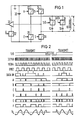
- the preferred embodiment utilizes the circuit illustrated in Figure 1 in the implanted device to transmit and receive information to and from an external device (not shown in Figure 1).
- An inductor or coil 10 is tuned to a first frequency f1 by a first capacitor 12 which is connected on one side thereof to one side of the inductor 10, and on the other side thereof to one side of a semiconductor switch 14.
- the other side of the semiconductor switch 14 is connected to the other side of the inductor 10, and it will be appreciated that when the switch 14 is closed, the first capacitor 12 will be connected in parallel with the inductor 10.
- the circuit will resonate at the first frequency f1 in an essentially sinusoidal fashion, with a slowly decaying sinusoidal voltage V L across the inductor 10.
- the semiconductor switch 14 may be a transmission gate type device.
- the switch 14 During transmission of data from the implanted device to the external device, the switch 14 is turned on or closed controlled by an input signal which is of high or true logic value, and which indicated that data is to be transmitted from the internal device to the external device. When data is to be received by the implanted device from the external device, the switch 14 will be turned off or opened.
- the device may be tuned to a second frequency f2 which is lower than the first frequency f1 and which may be realized by installing a second capacitor 16 in parallel across the first capacitor 12 and the inductor 10.
- One side of the second capacitor 16 is connected to the one side of the inductor 10, and the other side of the second capacitor 16 is connected to a second switch 18.
- the other side of the second switch 18 is connected to the other side of the inductor 10.
- the second switch 18 may be opened and closed to transmit binary data; in the embodiment discussed herein, for example, the second switch 18 will be turned on or closed when the data is to be serially transmitted is a logical "1", and turned off or opened when the data to be serially transmitted is a logical "0".
- the circuit will resonate at the second frequency f2 in an essentially sinusoidal fashion, also with a slowly decaying sinusoidal voltage V L across the inductor 10.
- the semiconductor switch 18 may also be a transmission gate type device.
- a first bridge switch 22 is connected on one side thereof to one side of the power source 20, and on the other side thereof to the other side of the inductor 10.
- a second bridge switch 24 is connected on one side thereof to the one side of the power source 20, and on the other side thereof to the one side of the inductor 10.
- a third bridge switch 26 is connected on one side thereof to the other side of the power source 20, and on the other side thereof to the other side of the inductor 10.
- a fourth bridge switch 28 is connected on one side thereof to other side of the power source 20, and on the other side thereof to the one side of the inductor 10.
- the four bridge switches 22, 24, 26, and 28 are turned off or opened most of the time.
- the four bridge switches 22, 24, 26, and 28 are operated by control signals A, B, c, and D, respectively.
- the first and fourth switches 22 and 28 are briefly closed.
- V L approximately reaches negative peaks
- the second and third switches 24 and 26 are briefly closed. In this way, a permanent oscillation of the tuned circuit at virtually constant amplitude is maintained.
- the first and second switches 22 and 24 may be P-MOS transistors, and the third and fourth switches 26 and 28 may be N-MOS transistors.
- the first and second switches 22 and 24 are then open when their relative control signals A and B are a logical "1" and closed when their relative control signals are a logical "0".
- the third and fourth switches 26 and 28 are open when their relative control signals c and D are a logical "0" and closed when their relative control signals are a "1".
- the signal V L has a constant frequency, either the first frequency f1 or the second frequency f2, during each bit internal.
- the first frequency f1 is 8192 Hz and the second frequency f2 is 4096 Hz.
- Their difference, 8192 Hz minus 4096 Hz, is 4096 Hz, which is half the bit rate of 8192 BPS.
- the second frequency is selected to be equal to the first frequency minus half the signaling bit rate f R , which is the reciprocal of the bit duration T.
- the supply of electrical energy to the circuit in brief pulses during both positive and negative voltage peaks, as opposed to a supply in pulse mode during only either positive or negative peaks, has the advantage of reducing distortion of the fundamental 8192 Hz or 4096 Hz sine waves. Lower distortion of course yields higher power efficiency, since the distortion is comprised of harmonics which will be discarded by the receiver (not shown in Figures 1 or 2).
- the second capacitor 16 While a data "0" is transmitted by the implanted device, the second capacitor 16 is disconnected by the second switch 18. However, the charge (or voltage) is stored on the second capacitor 16, and is reused when the next data "1" is transmitted because the V L polarity at the beginning of a bit to the beginning of the next consecutive bit never changes if a data "0" is transmitted. This important characteristic of the driving circuit provides that the circuit does not draw additional energy due to the transition in transmission
- the implanted device can also receive information from an external device which inductively couples signal into the inductor 10.
- the "DATA" input control to the second switch 18 is turned low, opening the second switch 18, and the T/ R input control to the switch 14 is turned low, opening the switch 14 and closing the first bridge switch 22 (see Figure 1, and also Figure 3, signal A).
- This configuration couples the inductor 10 to an implanted receiver 30, whose output is a binary signal available to be used to decode the information received from the external device.
- a switch 32 will provide power to the receiver 30 only during periods when the receive function is being implemented.
- the control signal G generated by the circuit of Figure 3, is provided to control the switch 32.
- the T/ R signal must be switched high and low only immediately before bit transition times. This ensures that no charge on the first capacitor 12 or on the second capacitor 16 is lost, since after a receive period the transmit period will start with the same V L polarity as that left from the prior transmission period.
- the circuit of Figure 3 does not require further explanation as it is common for those skilled in the art and may be implemented in a number of different ways.
- Figure 3 illustrates one possible example of a circuit which may be used to generate the control signals A, B, C, and D, and also to generate an additional control signal G.
- Inputs to the circuit of Figure 3 are the transmit/receive line T/ R which is also the input for the switch 14, the data line DATA which is also the input for the second switch 18, and three clock signals at 32768 Hz, 16384 Hz, and 8192 Hz.
- the source of the 32768 Hz signal may be derived from the crystal oscillator which is usually an integral part of implantable devices, as are the divided down frequencies of 16384 Hz, 8192 Hz, and 4096 Hz (used in Figure 5).
- the control signal G is used to operate a receiver in the implanted device, and will be discussed below.
- the transmit/receive line T/ R is the input for a first inverter 40, the output of which is the control signal G.
- the control signal G is also supplied as an input to a first two input NOR gate 42, to a first three input NOR gate 44, to a second three input NOR gate 46, and to a second two input NOR gate 48.
- the line and the 8192 Hz clock signal are the inputs for an AND gate 50, the output of which is an input for the first two input NOR gate 42.
- the output of the first two input NOR gate 42 is supplied as an input to both the J and K lines of a JK flip-flop 52, and the 16384 Hz clock signal is supplied to the JK flip-flop 52 as the clock signal.
- the Q output of the JK flip-flop 52 which is shown in the timing charts of Figure 2 as the control signal F, is supplied as an input to the D line of a D flip-flop 54, and as an input to a two input EXOR gate 56 and to the first three input NOR gate 44.
- the Q output of the JK flip-flop 52 is supplied as an input to the second three input NOR gate 46.
- the 32768 Hz clock signal is supplied as the clock signal to the D flip-flop 54, and the Q output of the D flip-flop 54 is supplied as an input to the two input EXOR gate 56.
- the output of the two input EXOR gate 56 which is shown in the timing charts of Figure 2 as the control signal E, is supplied as an input to the first three input NOR gate 44 and to the second three input NOR gate 46.
- the output of the first three input NOR gate 44 is the control signal D, and this output is supplied as an input to the second two input NOR gate 48.
- the output of the second two input NOR gate 48 is the control signal A.
- the output of the second three input NOR gate 46 is the control signal C, and this output is supplied as an input to a second inverter 58.
- the output of the second inverter 58 is the control signal B.
- a coil or inductor 60 is applied to the surface of the skin over the location of the inductor 10 of the implanted device.
- the two inductors 10 and 60 are constructed so that they will magnetically couple to each other. They may be regarded as two coils of a transformer having a low coupling coefficient.
- a double pole, double throw switch is utilized in the external transceiver to switch between transmit and receive functions.
- Such a switch which may be achieved either mechanically or electronically, is shown in Figure 4 in schematic form as a first double pole switch 62 which is mechanically connected to and operating with a second double pole switch 64.
- Each of the double pole switches 62 and 64 has a switching contact "a" which is electrically connected to a contact"b" when the switches 62 and 64 are in a first position, and which is electrically connected to a contact "c" when the double pole switches 62 and 64 are in a second position.
- the contact “c" of the first double pole switch 62 is connected to one side of the inductor 60.
- the contact “b” of the first double pole switch 62 and the contact “c” of the second double pole switch 64 are connected to the other side of the inductor 60.
- the contact “b” of the second double pole switch 64 is not used.
- the contact "a” of the first double pole switch 62 is connected to an input amplifier 66, the output of which is filtered by a bandpass filter 68 and then supplied to a decoder 70.
- the contact "c" of the second double pole switch 64 is connected to the output of a wave generator 72, which has as its input information supplied from an encoder 74.
- Information to be transmitted from the external transceiver to the implanted device is supplied to the encoder 74, which encodes the information and supplied it to the wave generator 72.
- the wave generator 72 then supplies a waveform containing the encoded information. It will be appreciated by those skilled in the art that the wave generator 72 may function as does the circuit of Figure 1 taught in this specification, or in other suitable ways known in the art.
- the inductor 60 When the double pole switches 62 and 64 are in the first position, the inductor 60 will be connected to the amplifier 66, and the external transceiver will act as a receiver.
- the voltage on the inductor 60 will be a replica of the signal V L on the inductor 10 of the implanted device ( Figure 1), but with a lower voltage amplitude due to the low coupling coefficient between the inductor 10 and the inductor 60.
- this signal is amplified by the amplifier 66 and goes through the bandpass filter 68, it goes into the decoder 70, which looks at the signal morphology for the presence of the first or second frequencies f1 or f2, thereby deciding whether each bit interval of the transmission is a zero or a one.
- Decoder circuits may be categorized as either coherent decoders or noncoherent decoders.
- Coherent decoders typically utilize phase locked loops or similar circuits to regenerate the two transmitted frequencies, and perform a correlation between these two frequencies and the received signal to decode the received signal.
- Noncoherent decoders are simpler, as they do not require a regeneration of the two transmitted frequencies. However, they require a higher signal-to-noise ratio in the received signal, which in turn requires higher implanted device transmitted power which is less desirable for use with a battery-powered implanted device. For the same transmitted power a coherent receiver will also provide a greater range, thereby allowing a larger distance between implanted and external inductor coils.
- a discussion of the coherent decoder is found in "Coherent Demodulation of Frequency Shift Keying with Low Deviation Ratio," R. DeBuda, IEEE Transactions on Communication , June 1972.
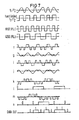
- FIG 5 An example of a coherent decoder is shown in Figure 5, which has as its input the amplified and filtered signal received from the implanted device. It is useful to discuss the operation of the coherent decoder in conjunction with an example of the transmission and receiving of data, and such an example is shown in Figures 6 and 7.
- Figure 6 a sample stream of data to be transmitted by the implanted device shown in Figure 1 to the external transceiver shown in Figure 4 is illustrated as DATA IN. This data may be thought of as the result of adding two streams of data, one with odd bits dI and the other with even bits dg.
- the implanted device will transmit trains of two frequencies f1 and f2, as described above in conjunction with Figure 1.
- the trains of frequencies f1 and f2 may be analytically viewed as a simultaneous transmission of two quadrature carriers (carriers having a 90-degree relative phase shift), with each binary phase being shift keyed or modulated by the data to be transmitted.
- the odd bits dI will modulate one carrier and the even bits d Q will modulate the other carrier.
- the second frequency f2 is selected to be equal to the first frequency f1 minus half the signaling bit rate f R , which is the reciprocal of the bit duration T.
- the signaling bit rate f R of the preferred embodiment is 8192 BPS
- the first frequency f1 is 8192 Hz
- the second frequency f2 is 4096 Hz, with the difference between f1 and f2 being 4096 Hz, which is half the signaling bit rate f R of 8192 BPS.
- the frequency of the two carriers f1 and f2 can be trigonometrically demonstrated to be the arithmetic f1 and f2 average, which in this case is 6144 Hz.
- the advantage of this method lies in the fact that each bit now lasts 2T and the receiver has twice the time to make a decision whether the bit transmitted was a 0 or a 1, and as such is able to reject more noise.
- the transmitter need not be implemented as a two quadrature component system; only the receiver must be so constructed.
- Figure 6 demonstrates how the two modulated 6144 Hz carriers I and Q are together equivalent to the f1/f2 train.
- the I (in-phase) and Q (quadrature) signals are also amplitude modulated with a maximum in the middle of each odd bit d I or even bit d Q .
- the amplified and filtered f1/f2 signal received by the external transceiver is supplied to a hard limiter 76, the operation of which is known to those skilled in the art. Its output, the hard-limited f1/f2 signal, has two binary states, positive or negative, according to polarity of the amplified and filtered f1/f2 signal.
- This hard-limited f1/f2 signal is supplied to two multipliers, namely an I multiplier 78, and a Q multiplier 80.
- the function of the I multiplier 78 is to isolate the I (in-phase) component of the hard-limited f1/f2 signal
- the function of the Q multiplier 80 is to isolate the Q (Quadrature) component of the hard-limited f1/f2 signal.
- the hard-limited f1/f2 signal is also supplied to a phase-locked-loop circuit 82, where it is used to synchronize the clock signals provided as outputs from the phase-locked-loop circuit 82.
- the phase-locked-loop circuit 82 looks at the zero crossings of hard-limited f1/f2 signal and adjusts the phase of its 4096 Hz, 8192 Hz, and 16384 Hz outputs to match the phase relationship of the received f1/f2 received by the external transceiver.
- the phase-locked-loop circuit 84 is not difficult to implement due to the special relations selected between the first frequency f1, the second frequency f2 , and the signaling bit rate f R which is the reciprocal of the bit duration T, namely that the second frequency f2 is one-half the first frequency f1, and that the first frequency f1 equal to the bit signaling rate f R .
- the f and i signals have to be generated by the receiver.
- Two modulated recovered carriers are generated by adding and subtracting the 8192 Hz and the 4096 Hz outputs from the phase-locked-loop circuit 82 together.
- a first summer 84 adds the 8192 Hz and the 4096 Hz outputs from the phase-locked-loop circuit 82 together to produce the modulated recovered I carrier f, which is shown in Figure 7 together with the sinusoidal I carrier labeled as g for comparison.
- a second summer 86 subtracts the 8192 Hz output of the phase-locked-loop circuit 82 from the 4096 Hz output of the phase-locked-loop circuit 82 to produce the modulated recovered Q carrier i, which is shown in Figure 7 together with the sinusoidal Q carrier labeled as j for comparison.
- the I multiplier 78 multiplies the hard-limited f1/f2 signal by the modulated recovered I carrier f to isolate the I (in-phase) component of the hard-limited f1/f2 signal.
- the sign of the modulated recovered I carrier f is either changed if the hard-limited f1/f2 signal is negative or unchanged if the hard-limited f1/f2 signal is positive.
- the resulting signal which is supplied as the output of the I multiplier 78 is the signal k, shown in Figure 7, which signal k is supplied to an integrate-and-dump device 88.
- the Q multiplier 80 multiplies the hard-limited f1/f2 signal by the modulated recovered Q carrier carrier i to to isolate the Q (quadrature) component of the hard-limited f1/f2 signal.
- the sign of the modulated recovered Q carrier i is either changed if the hard-limited f1/f2 signal is negative or unchanged if the hard-limited f1/f2 signal is positive.
- the resulting signal which is supplied as the output of the Q multiplier 80 is the signal m, shown in Figure 7, which signal m is supplied to an integrate-and-dump device 90.
- the 4096 Hz clock output of the phase-locked-loop circuit 82 is supplied as an input to the D line on a D flip-flop 92.
- the 16384 Hz clock output of the phase-locked-loop circuit 82 is supplied as the clock input to the D flip-flop 92 to regenerate the data bit clock thereof.
- the Q and Q outputs of the D flip-flop 92 are therefore a series of alternating 1's and 0's, with the period in which one 1 and one 0 occurs being 2T.
- the D flip-flop 92 may be seen as a sort of steering circuit, which alternately causes signals from the in-phase side and the quadrature side of the circuit of Figure 5 to be combined to produce a single consolidated output.
- the Q output of the D flip-flop 92 is connected to one side of a capacitor 94, the other side of which is connected to the integrate-and-dump device 88.
- a resistor 96 is connected on one side to ground, and on the other side to the other side of the capacitor 94.
- the capacitor 94 and the resistor 96 provide to the integrate-and-dump device 88 a series of pulses which occur shortly after the rising edges of the Q output of the D flip-flop 92.
- the integrate-and-dump device 88 integrates the k signal, and at the occurrence of each pulse occurring after a rising edge of the Q output of the D flip-flop 92, the integrate-and-dump device 88 is reset.
- the output of the D flip-flop 92 is connected to one side of a capacitor 98, the other side of which is connected to the integrate-and-dump device 90.
- a resistor 100 is connected on one side to ground, and on the other side to the other side of the capacitor 98.
- the capacitor 98 and the resistor 100 provide to the integrate-and-dump device 90 a series of pulses which occur shortly after the rising edges of the Q output of the D flip-flop 92.
- the integrate-and-dump device 90 integrates the m signal, and at the occurrence of each pulse occurring after a rising edge of the Q output of the D flip-flop 92, the integrate-and-dump device 90 is reset.
- the integrate-and-dump devices 88 and 90 will produce an output reflecting the inputs thereto. If for the majority of the 2T period the input to one of the integrate-and-dump devices 88 and 90 is high, the output from that device at the end of the 2T period will be high. Similarly, if for the majority of the 2T period the input to one of the integrate-and-dump devices 88 and 90 is low, the output from that device at the end of the 2T period will be low.
- the integrate-and-dump devices 88 and 90 may thus be viewed as low-pass filters.
- the output from the integrate-and-dump device 88 is supplied as an input to the D line on a D flip-flop 102, which has as its clock input the Q output from the D flip-flop 92.
- the output from the integrate-and-dump device 88 is therefore sampled by the D flip-flop 102 after each period of time of 2T and at the rising edge of the Q output of the D flip-flop 92, which period is that determined by the D flip-flop 92.
- the Q output from the D flip-flop 102 is the signal 1 shown in Figure 7.
- the output from the integrate-and-dump device 90 is supplied as an input to the D line on a D flip-flop 104, which has as its clock input the Q output from the D flip-flop 92.
- the output from the integrate-and-dump device 90 is therefore sampled by the D flip-flop 104 after each period of time of 2T and at the rising edge of the Q output of the D flip-flop 92, which period is that determined by the D flip-flop 92.
- the Q output from the D flip-flop 104 is the signal n shown in Figure 7.
- the integrate and dump cycles of the integrate-and-dump device 88 and the integrate-and-dump device 90 and the flip-flop samples of the D flip-flop 102 and the D flip-flop 104 are alternating, and must be interleaved to produce a single output from the external transceiver reflecting the input from the implanted device. Accordingly, the Q output 1 from the D flip-flop 102 and the Q output n from the D flip-flop 104 are supplied as inputs to a two input EXOR gate 106, the output of which is the desired received data. It will be appreciated that the data output from the two input EXOR gate 106 shown in Figure 7 will be time delayed by a period of 2T from the data input shown in Figure 6. This delay is caused by the sampling of the integrate-and-dump devices 88 and 90 by the D flip-flops 102 and 104, respectively, once every period of 2T.
- Noncoherent decoders which are essentially envelope detectors, are well known in the art, but they would not work as well as coherent decoders at the relatively data frequency used herein. Because a coherent decoder has two parallel paths, and each path has a two bit interval (2T) to integrate the signal, a coherent decoder will necessarily have a better performance than the noncoherent decoder, and will be significantly more resistant to noise.
- the system of the present invention achieves a reliable high rate of data transmission at a high signal to noise ratio, while requiring only low transmitter power, features which are very important for an implantable device.
- the signal is received using only a relatively small bandwidth, thereby both reducing noise and permitting operation of the transmitter at lower power.
- the maximum bit rate may be equal to the first frequency, a feature not possible in prior art systems, since in such systems in order to detect an amplitude modulated signal it required more than one period (typically more than four periods) of the carrier.
- a maximum speed of approximately eight kBPS may be achieved.
- the system of the present invention is capable of accurately transmitting and receiving data at a rate which enables the substantial amounts of data used by current implantable systems to be conveniently sent in a relatively short period of time.
- the amount of power required by the implanted portion of the system is minimal, thereby extending battery life, and the system of the present invention is quite compact. While attaining these advantages and features, no relative disadvantage is incurred.
Abstract
Description
- - The present invention relates generally to a telemetry system for use in medical devices of various types and for various purposes implantable within the human body, and more particularly to a telemetry system which will transmit data at a relatively high rate in both directions while retaining a high degree of accuracy.
- With the ever-shrinking size of electronic circuitry, the implantation into the human body of electronic medical devices has become more and more common. Although the most commonly known of such devices is the cardiac pacemaker, there are a variety of devices which are implanted into the human body, including devices for the stimulation or tenting, or both, of the brain, nerves, the spinal cord, muscles, bones, glands, or other body organs or tissues.
- It will be appreciated by those skilled in the art that such implantable devices are becoming increasingly complex, and that more functions can be crammed into a relatively smaller electronic chip or circuit. Implantable medical devices have used bidirectional telemetry for a number of years. Information transmitted between the implanted device and an external transceiver may include, for example, device identification information, biological data, current operational parameters of of the device, technical information regarding proper operation of the device, battery charge condition, revised operational parameters (programming information) for the device, and verification of information transmitted between the implanted device and the external transceiver.
- With an ever-increasing amount of data being processed and available within the implantable device, there has been an corresponding increase in the need to transmit more data from the implanted device to the external transceiver for analysis, reprogramming of the implantable device, or other purposes. The need for more data to be transmitted in both directions has increased tremendously the amount of time required both to interrogate the implanted device and to reprogram the implanted device. An upper limit on the amount of data flowing between the implanted device and the external transceiver has therefore become directly proportional to the amount of time which may reasonably taken to interrogate and reprogram the implanted device.
- Accordingly, it is desirable to achieve a higher rate of data transfer between the implanted device and the external transceiver to eliminate this artificial impediment and to maximize the communication between the implanted device and the external transceiver. Of course, an increase in the rate of data exchange may not be obtained at the expense of accuracy in a medical device, particularly if the device is a life-sustaining device such as a pacemaker. Absolute accuracy is required, and it is apparent that an increase in the rate of data transfer will be nullified by an increase in the amount of time spent to verify data to ensure the degree of accuracy required.
- The recent development of LSI circuits incorporating low current analog-to-digital converters has made the use of such converters in implantable devices possible. There are, of course, limitations surrounding the design of new implantable systems or portions thereof, the most limiting of which is the consumption of energy by the system. Implanted systems are customarily powered by a long-lasting non-replaceable internal battery, and the current consumption of a telemetry sub-system thus becomes perhaps the most important design factor to be considered.
- Previously known devices have established various methods of communicating non-invasively through the skin. For example, U.S. Patent No. 4,223,679, to Schulman et al., which patent is assigned to the assignee of the present invention, shows an implanted device which uses little or no current to transmit information by relying on reflected impedance of an internal L-C circuit. Internal modulation circuits in the implanted device transmit digital or analog data by modulating the reflected impedance, and the external transceiver utilizes an oscillator having varying frequency and amplitude outputs determined by a coupled RF magnetic field carrier to an L-C circuit in the external transceiver. This system works well, but, unfortunately, has speed limitations making it unsuitable for transmitting the amount of information contemplated herein.
- Another type of device uses an active type transmitter, with the transmitted energy being taken from the implantable device battery. This type of device, which is illustrated in U.S. Patent No. 4,281,664, to Duggan, has a data rate which is limited to approximately 100 BPS (bits per second). Another device which utilizes an active type transmitter is shown in U.S. Patent No. 4,453,162, to Daly et al. The Daly et al. device can not achieve more than 0.25 to 0.05 bps/carrier cycle, a rate too low for the applications contemplated herein.
- Those skilled in the art will also appreciate that it is not practical to increase the carrier frequency above approximately eight kHz, since the metal enclosure of the implanted device will experience eddy currents great enough to attenuate the signal significantly. In addition, increasing the carrier frequency makes electromagnetic interference from video display terminals, which are generally approximately 16 kHz, a significant problem. Consequently, techniques requiring a number of carrier cycles for each signal bit will be capable of achieving a speed only two to four kBPS.
- It will therefore be appreciated that there exists a substantial need for a telemetry system which is capable of accurately transmitting and receiving data at a rate enabling the substantial amounts of data used by current implantable systems to be conveniently sent in a relatively short period of time. The amount of power required by the implanted portion of the system must be minimal, so as not to adversely affect battery life. Finally, the system should be compact so as to not add significantly to the space required by the implanted device.
- The disadvantages and limitations of the background art discussed above are overcome by the present invention. With this invention, a circuit using an active transmitter can achieve a bit rate equal to or higher than the carrier frequency, thereby achieving a practical speed of about eight kBPS. Also, the circuit of the present invention uses a drive circuit which achieves high power efficiency.
- In accordance with the present invention an inductor in the implantable device is used to generate a magnetic field through which information may be transmitted to an external receiver. The inductor is then tuned to one of two frequencies by using either one or two capacitors connected in parallel across the inductor. While transmitting data, one of the capacitors is permanently connected in parallel across the inductor, and determines the first resonant frequency of the system.
- One side of the second capacitor is connected to one side of the parallel first capacitor and inductor combination; the other side of the second capacitor is connected to one side of a switch, the other side of which switch is connected to the other side of the parallel first capacitor and inductor combination. Whenever the switch is closed, the second capacitor will be connected in parallel together with the first capacitor and the inductor, and the resulting tuned circuit will resonate at a second frequency.
- The external transceiver will contain means for decoding the first and second frequency carriers and for recovering the original data which was coded and transmitted. It will be understood that the process may be reversed to transmit data from the external transceiver to the implanted device.
- In the preferred embodiment, the second frequency is selected to be equal to the first frequency minus half the signaling bit rate. The switch is controlled such that it is open when a "0" is to be transmitted, and closed when a "1" is to be transmitted, with the switch position being changed at the bit boundaries. The tuned circuit is energized for a short period of time each time its voltage reaches a positive or a negative peak by connecting it at the right polarity to the implanted device power source. The bit rate is chosen such that during a bit interval the tuned circuit voltage has an excursion of an integer number of peak-to-peak voltages.
- By energizing the tuned circuit while its voltage passes through positive and negative peaks, as opposed to energizing it during only one polarity peak, sine wave distortion is reduced and the higher harmonic content, which is synonymous with lost energy, is reduced, thereby increasing transmitter power efficiency. In addition, as will become apparent from the following description, the method of switching between the first and second frequencies allows a constant amplitude carrier to be transmitted, as opposed to pulsing a carrier on and off, or abruptly changing the carrier phase.
- The system of the present invention thereby achieves a reliable transmission at a higher signal to noise ratio, and at an implicitly lower average transmitter power, which features are very important for an implantable device. Also, by avoiding sharp amplitude and phase changes, the signal may be received by using only a relatively small bandwidth, which in turn both reduces the noise and permits operation of the transmitter at lower power. The maximum bit rate may therefore be equal to the first frequency. This was not possible in prior art systems, for in order to detect an amplitude modulated signal it requires more than one period (typically more than four periods) of the carrier.
- Similarly, phase modulation as illustrated in the Daly et al. reference, cited above, will not achieve a bit rate equal to the first frequency. Thus, by energizing the tuned circuit during both positive and negative voltage excursions and by having the two tuning capacitors connected to the inductor, a maximum speed of approximately eight kBPS may be achieved. The system of the present invention is thereby capable of accurately transmitting and receiving data at a rate which enables the substantial amounts of data used by current implantable systems to be conveniently sent in a relatively short period of time. The amount of power required by the implanted portion of the system is minimal, thereby extending battery life. The system of the present invention is also quite compact, thereby fitting conveniently in the small space afforded by the implanted device. All of the above advantages are obtained without any relative disadvantage, making the system of the present invention a highly desirable improvement to the art.
- These and other advantages of the present invention are best understood with reference to the drawings, in which:
- Figure 1 is an electrical schematic of the implanted transceiver driver circuit of the present invention:
- Figure 2 is a timing diagram of control and output signals for the circuit shown in Figure 1;
- Figure 3 is an electrical schematic of a circuit which may be used to generate the control signals shown in Figure 2:
- Figure 4 is a functional schematic of the external transceiver for use with the implanted transceiver shown in Figure 1;
- Figure 5 is a functional schematic of a coherent decoder which may be used in the circuit of Figure 4;
- Figure 6 is a diagram showing the data and output signals generated and transmitted by the implanted transceiver shown in Figure 1; and
- Figure 7 is a diagram of signals generated by the coherent decoder of Figure 5 which are used to decode the received signal of Figure 6.
- The preferred embodiment utilizes the circuit illustrated in Figure 1 in the implanted device to transmit and receive information to and from an external device (not shown in Figure 1). An inductor or coil 10 is tuned to a first frequency f₁ by a
first capacitor 12 which is connected on one side thereof to one side of the inductor 10, and on the other side thereof to one side of asemiconductor switch 14. The other side of thesemiconductor switch 14 is connected to the other side of the inductor 10, and it will be appreciated that when theswitch 14 is closed, thefirst capacitor 12 will be connected in parallel with the inductor 10. The circuit will resonate at the first frequency f₁ in an essentially sinusoidal fashion, with a slowly decaying sinusoidal voltage VL across the inductor 10. Thesemiconductor switch 14 may be a transmission gate type device. - During transmission of data from the implanted device to the external device, the
switch 14 is turned on or closed controlled by an input signal which is of high or true logic value, and which indicated that data is to be transmitted from the internal device to the external device. When data is to be received by the implanted device from the external device, theswitch 14 will be turned off or opened. - The device may be tuned to a second frequency f₂ which is lower than the first frequency f₁ and which may be realized by installing a
second capacitor 16 in parallel across thefirst capacitor 12 and the inductor 10. One side of thesecond capacitor 16 is connected to the one side of the inductor 10, and the other side of thesecond capacitor 16 is connected to asecond switch 18. The other side of thesecond switch 18 is connected to the other side of the inductor 10. Thesecond switch 18 may be opened and closed to transmit binary data; in the embodiment discussed herein, for example, thesecond switch 18 will be turned on or closed when the data is to be serially transmitted is a logical "1", and turned off or opened when the data to be serially transmitted is a logical "0". When thesecond switch 18 is closed, the circuit will resonate at the second frequency f₂ in an essentially sinusoidal fashion, also with a slowly decaying sinusoidal voltage VL across the inductor 10. Thesemiconductor switch 18 may also be a transmission gate type device. - Four semiconductor switches are connected as a bridge circuit to a
power source 20, which is typically the battery powering the implanted device. Afirst bridge switch 22 is connected on one side thereof to one side of thepower source 20, and on the other side thereof to the other side of the inductor 10. Asecond bridge switch 24 is connected on one side thereof to the one side of thepower source 20, and on the other side thereof to the one side of the inductor 10. Athird bridge switch 26 is connected on one side thereof to the other side of thepower source 20, and on the other side thereof to the other side of the inductor 10. Finally, afourth bridge switch 28 is connected on one side thereof to other side of thepower source 20, and on the other side thereof to the one side of the inductor 10. - It will be appreciated that the four
bridge switches bridge switches fourth switches third switches - For example, the first and
second switches fourth switches second switches fourth switches - Referring now to Figure 2 in conjunction with Figure 1, it is apparent that the signal VL has a constant frequency, either the first frequency f₁ or the second frequency f₂, during each bit internal. In the preferred embodiment the first frequency f₁ is 8192 Hz and the second frequency f₂ is 4096 Hz. Their difference, 8192 Hz minus 4096 Hz, is 4096 Hz, which is half the bit rate of 8192 BPS.
- In the preferred embodiment, the second frequency is selected to be equal to the first frequency minus half the signaling bit rate fR, which is the reciprocal of the bit duration T. By selecting these frequencies, during each bit interval the voltage VL on the inductor 10 will start and stop on a peak value. The average current drawn from the
power source 20 is very small, since during each supplying pulse the tuned circuit amplitude has to be increased only slightly to compensate for the natural decay in amplitude due to the limited quality factor (Q) of the coil. - The supply of electrical energy to the circuit in brief pulses during both positive and negative voltage peaks, as opposed to a supply in pulse mode during only either positive or negative peaks, has the advantage of reducing distortion of the fundamental 8192 Hz or 4096 Hz sine waves. Lower distortion of course yields higher power efficiency, since the distortion is comprised of harmonics which will be discarded by the receiver (not shown in Figures 1 or 2).
- While a data "0" is transmitted by the implanted device, the
second capacitor 16 is disconnected by thesecond switch 18. However, the charge (or voltage) is stored on thesecond capacitor 16, and is reused when the next data "1" is transmitted because the VL polarity at the beginning of a bit to the beginning of the next consecutive bit never changes if a data "0" is transmitted. This important characteristic of the driving circuit provides that the circuit does not draw additional energy due to the transition in transmission - The implanted device can also receive information from an external device which inductively couples signal into the inductor 10. During receiving, the "DATA" input control to the
second switch 18 is turned low, opening thesecond switch 18, and the T/R input control to theswitch 14 is turned low, opening theswitch 14 and closing the first bridge switch 22 (see Figure 1, and also Figure 3, signal A). This configuration couples the inductor 10 to an implantedreceiver 30, whose output is a binary signal available to be used to decode the information received from the external device. - Optionally, a switch 32 will provide power to the
receiver 30 only during periods when the receive function is being implemented. The control signal G, generated by the circuit of Figure 3, is provided to control the switch 32. It should be noted that the T/R signal must be switched high and low only immediately before bit transition times. This ensures that no charge on thefirst capacitor 12 or on thesecond capacitor 16 is lost, since after a receive period the transmit period will start with the same VL polarity as that left from the prior transmission period. Beyond this, the circuit of Figure 3 does not require further explanation as it is common for those skilled in the art and may be implemented in a number of different ways. - Figure 3 illustrates one possible example of a circuit which may be used to generate the control signals A, B, C, and D, and also to generate an additional control signal G. Inputs to the circuit of Figure 3 are the transmit/receive line T/
R which is also the input for theswitch 14, the data line DATA which is also the input for thesecond switch 18, and three clock signals at 32768 Hz, 16384 Hz, and 8192 Hz. The source of the 32768 Hz signal may be derived from the crystal oscillator which is usually an integral part of implantable devices, as are the divided down frequencies of 16384 Hz, 8192 Hz, and 4096 Hz (used in Figure 5). The control signal G is used to operate a receiver in the implanted device, and will be discussed below. - The transmit/receive line T/
R is the input for afirst inverter 40, the output of which is the control signal G. The control signal G is also supplied as an input to a first two input NORgate 42, to a first three input NORgate 44, to a second three input NORgate 46, and to a second two input NORgate 48. The line and the 8192 Hz clock signal are the inputs for an ANDgate 50, the output of which is an input for the first two input NORgate 42. The output of the first two input NORgate 42 is supplied as an input to both the J and K lines of a JK flip-flop 52, and the 16384 Hz clock signal is supplied to the JK flip-flop 52 as the clock signal. - The Q output of the JK flip-
flop 52, which is shown in the timing charts of Figure 2 as the control signal F, is supplied as an input to the D line of a D flip-flop 54, and as an input to a twoinput EXOR gate 56 and to the first three input NORgate 44. TheQ output of the JK flip-flop 52 is supplied as an input to the second three input NORgate 46. The 32768 Hz clock signal is supplied as the clock signal to the D flip-flop 54, and the Q output of the D flip-flop 54 is supplied as an input to the twoinput EXOR gate 56. - The output of the two
input EXOR gate 56, which is shown in the timing charts of Figure 2 as the control signal E, is supplied as an input to the first three input NORgate 44 and to the second three input NORgate 46. The output of the first three input NORgate 44 is the control signal D, and this output is supplied as an input to the second two input NORgate 48. The output of the second two input NORgate 48 is the control signal A. The output of the second three input NORgate 46 is the control signal C, and this output is supplied as an input to asecond inverter 58. The output of thesecond inverter 58 is the control signal B. - The external transceiver used to receive data transmitted from the implanted device and to transmit data to the implanted device may now be discussed in conjunction with Figure 4. A coil or
inductor 60 is applied to the surface of the skin over the location of the inductor 10 of the implanted device. The twoinductors 10 and 60 are constructed so that they will magnetically couple to each other. They may be regarded as two coils of a transformer having a low coupling coefficient. - A double pole, double throw switch is utilized in the external transceiver to switch between transmit and receive functions. Such a switch, which may be achieved either mechanically or electronically, is shown in Figure 4 in schematic form as a first
double pole switch 62 which is mechanically connected to and operating with a seconddouble pole switch 64. Each of the double pole switches 62 and 64 has a switching contact "a" which is electrically connected to a contact"b" when theswitches - The contact "c" of the first
double pole switch 62 is connected to one side of theinductor 60. The contact "b" of the firstdouble pole switch 62 and the contact "c" of the seconddouble pole switch 64 are connected to the other side of theinductor 60. The contact "b" of the seconddouble pole switch 64 is not used. The contact "a" of the firstdouble pole switch 62 is connected to aninput amplifier 66, the output of which is filtered by abandpass filter 68 and then supplied to adecoder 70. - The contact "c" of the second
double pole switch 64 is connected to the output of awave generator 72, which has as its input information supplied from anencoder 74. Information to be transmitted from the external transceiver to the implanted device is supplied to theencoder 74, which encodes the information and supplied it to thewave generator 72. Thewave generator 72 then supplies a waveform containing the encoded information. It will be appreciated by those skilled in the art that thewave generator 72 may function as does the circuit of Figure 1 taught in this specification, or in other suitable ways known in the art. When the double pole switches 62 and 64 are in the second position, information may be transmitted from the external transceiver using theinductor 60, which will be connected to thewave generator 72 when the double pole switches 62 and 64 are in the second position. - When the double pole switches 62 and 64 are in the first position, the
inductor 60 will be connected to theamplifier 66, and the external transceiver will act as a receiver. The voltage on theinductor 60 will be a replica of the signal VL on the inductor 10 of the implanted device (Figure 1), but with a lower voltage amplitude due to the low coupling coefficient between the inductor 10 and theinductor 60. After this signal is amplified by theamplifier 66 and goes through thebandpass filter 68, it goes into thedecoder 70, which looks at the signal morphology for the presence of the first or second frequencies f₁ or f₂, thereby deciding whether each bit interval of the transmission is a zero or a one. - Decoder circuits may be categorized as either coherent decoders or noncoherent decoders. Coherent decoders typically utilize phase locked loops or similar circuits to regenerate the two transmitted frequencies, and perform a correlation between these two frequencies and the received signal to decode the received signal. Noncoherent decoders are simpler, as they do not require a regeneration of the two transmitted frequencies. However, they require a higher signal-to-noise ratio in the received signal, which in turn requires higher implanted device transmitted power which is less desirable for use with a battery-powered implanted device. For the same transmitted power a coherent receiver will also provide a greater range, thereby allowing a larger distance between implanted and external inductor coils. A discussion of the coherent decoder is found in "Coherent Demodulation of Frequency Shift Keying with Low Deviation Ratio," R. DeBuda, IEEE Transactions on Communication, June 1972.
- An example of a coherent decoder is shown in Figure 5, which has as its input the amplified and filtered signal received from the implanted device. It is useful to discuss the operation of the coherent decoder in conjunction with an example of the transmission and receiving of data, and such an example is shown in Figures 6 and 7. In Figure 6, a sample stream of data to be transmitted by the implanted device shown in Figure 1 to the external transceiver shown in Figure 4 is illustrated as DATA IN. This data may be thought of as the result of adding two streams of data, one with odd bits dI and the other with even bits dg.
- The implanted device will transmit trains of two frequencies f₁ and f₂, as described above in conjunction with Figure 1. The trains of frequencies f₁ and f₂ may be analytically viewed as a simultaneous transmission of two quadrature carriers (carriers having a 90-degree relative phase shift), with each binary phase being shift keyed or modulated by the data to be transmitted. The odd bits dI will modulate one carrier and the even bits dQ will modulate the other carrier.
- As described above, in the preferred embodiment the second frequency f₂ is selected to be equal to the first frequency f₁ minus half the signaling bit rate fR, which is the reciprocal of the bit duration T. The signaling bit rate fR of the preferred embodiment is 8192 BPS, the first frequency f₁ is 8192 Hz, and the second frequency f₂ is 4096 Hz, with the difference between f₁ and f₂ being 4096 Hz, which is half the signaling bit rate fR of 8192 BPS.
- The frequency of the two carriers f₁ and f₂ can be trigonometrically demonstrated to be the arithmetic f₁ and f₂ average, which in this case is 6144 Hz. The advantage of this method lies in the fact that each bit now lasts 2T and the receiver has twice the time to make a decision whether the bit transmitted was a 0 or a 1, and as such is able to reject more noise. The transmitter need not be implemented as a two quadrature component system; only the receiver must be so constructed. Figure 6 demonstrates how the two modulated 6144 Hz carriers I and Q are together equivalent to the f₁/f₂ train. The I (in-phase) and Q (quadrature) signals are also amplitude modulated with a maximum in the middle of each odd bit dI or even bit dQ.
- Referring again to Figure 5, in conjunction with Figure 7, the amplified and filtered f₁/f₂ signal received by the external transceiver is supplied to a
hard limiter 76, the operation of which is known to those skilled in the art. Its output, the hard-limited f₁/f₂ signal, has two binary states, positive or negative, according to polarity of the amplified and filtered f₁/f₂ signal. This hard-limited f₁/f₂ signal is supplied to two multipliers, namely anI multiplier 78, and aQ multiplier 80. The function of theI multiplier 78 is to isolate the I (in-phase) component of the hard-limited f₁/f₂ signal, and the function of theQ multiplier 80 is to isolate the Q (Quadrature) component of the hard-limited f₁/f₂ signal. - The hard-limited f₁/f₂ signal is also supplied to a phase-locked-
loop circuit 82, where it is used to synchronize the clock signals provided as outputs from the phase-locked-loop circuit 82. The phase-locked-loop circuit 82 looks at the zero crossings of hard-limited f₁/f₂ signal and adjusts the phase of its 4096 Hz, 8192 Hz, and 16384 Hz outputs to match the phase relationship of the received f₁/f₂ received by the external transceiver. The phase-locked-loop circuit 84 is not difficult to implement due to the special relations selected between the first frequency f₁, the second frequency f₂ , and the signaling bit rate fR which is the reciprocal of the bit duration T, namely that the second frequency f₂ is one-half the first frequency f₁, and that the first frequency f₁ equal to the bit signaling rate fR. The f and i signals have to be generated by the receiver. - Two modulated recovered carriers are generated by adding and subtracting the 8192 Hz and the 4096 Hz outputs from the phase-locked-
loop circuit 82 together. Afirst summer 84 adds the 8192 Hz and the 4096 Hz outputs from the phase-locked-loop circuit 82 together to produce the modulated recovered I carrier f, which is shown in Figure 7 together with the sinusoidal I carrier labeled as g for comparison. Similarly, asecond summer 86 subtracts the 8192 Hz output of the phase-locked-loop circuit 82 from the 4096 Hz output of the phase-locked-loop circuit 82 to produce the modulated recovered Q carrier i, which is shown in Figure 7 together with the sinusoidal Q carrier labeled as j for comparison. - It should be noted that the signals f and i are approximations to the exact sinusoidal signals g and j, respectively. However, any performance degradation resulting from this approximation is negligible, and does not require further complicating the circuit of Figure 5 with filters to smooth the f and i signals into closer approximations of the g and j signals, respectively.
- The
I multiplier 78 multiplies the hard-limited f₁/f₂ signal by the modulated recovered I carrier f to isolate the I (in-phase) component of the hard-limited f₁/f₂ signal. When the hard-limited f₁/f₂ signal is multiplied by the modulated recovered I carrier f in theI multiplier 78, the sign of the modulated recovered I carrier f is either changed if the hard-limited f₁/f₂ signal is negative or unchanged if the hard-limited f₁/f₂ signal is positive. The resulting signal which is supplied as the output of theI multiplier 78 is the signal k, shown in Figure 7, which signal k is supplied to an integrate-and-dump device 88. - Similarly, the
Q multiplier 80 multiplies the hard-limited f₁/f₂ signal by the modulated recovered Q carrier carrier i to to isolate the Q (quadrature) component of the hard-limited f₁/f₂ signal. When the hard-limited f₁/f₂ signal is multiplied by the modulated recovered Q carrier i in theQ multiplier 80, the sign of the modulated recovered Q carrier i is either changed if the hard-limited f₁/f₂ signal is negative or unchanged if the hard-limited f₁/f₂ signal is positive. The resulting signal which is supplied as the output of theQ multiplier 80 is the signal m, shown in Figure 7, which signal m is supplied to an integrate-and-dump device 90. - The 4096 Hz clock output of the phase-locked-
loop circuit 82 is supplied as an input to the D line on a D flip-flop 92. The 16384 Hz clock output of the phase-locked-loop circuit 82 is supplied as the clock input to the D flip-flop 92 to regenerate the data bit clock thereof. The Q and Q outputs of the D flip-flop 92 are therefore a series of alternating 1's and 0's, with the period in which one 1 and one 0 occurs being 2T. The D flip-flop 92 may be seen as a sort of steering circuit, which alternately causes signals from the in-phase side and the quadrature side of the circuit of Figure 5 to be combined to produce a single consolidated output. - The Q output of the D flip-
flop 92 is connected to one side of acapacitor 94, the other side of which is connected to the integrate-and-dump device 88. Aresistor 96 is connected on one side to ground, and on the other side to the other side of thecapacitor 94. Thecapacitor 94 and theresistor 96 provide to the integrate-and-dump device 88 a series of pulses which occur shortly after the rising edges of the Q output of the D flip-flop 92. The integrate-and-dump device 88 integrates the k signal, and at the occurrence of each pulse occurring after a rising edge of the Q output of the D flip-flop 92, the integrate-and-dump device 88 is reset. - The output of the D flip-
flop 92 is connected to one side of acapacitor 98, the other side of which is connected to the integrate-and-dump device 90. Aresistor 100 is connected on one side to ground, and on the other side to the other side of thecapacitor 98. Thecapacitor 98 and theresistor 100 provide to the integrate-and-dump device 90 a series of pulses which occur shortly after the rising edges of theQ output of the D flip-flop 92. The integrate-and-dump device 90 integrates the m signal, and at the occurrence of each pulse occurring after a rising edge of theQ output of the D flip-flop 92, the integrate-and-dump device 90 is reset. - The integrate-and-
dump devices dump devices dump devices dump devices - The output from the integrate-and-
dump device 88 is supplied as an input to the D line on a D flip-flop 102, which has as its clock input the Q output from the D flip-flop 92. The output from the integrate-and-dump device 88 is therefore sampled by the D flip-flop 102 after each period of time of 2T and at the rising edge of the Q output of the D flip-flop 92, which period is that determined by the D flip-flop 92. The Q output from the D flip-flop 102 is thesignal 1 shown in Figure 7. - Likewise, the output from the integrate-and-
dump device 90 is supplied as an input to the D line on a D flip-flop 104, which has as its clock input theQ output from the D flip-flop 92. The output from the integrate-and-dump device 90 is therefore sampled by the D flip-flop 104 after each period of time of 2T and at the rising edge of theQ output of the D flip-flop 92, which period is that determined by the D flip-flop 92. The Q output from the D flip-flop 104 is the signal n shown in Figure 7. - It will be appreciated that the integrate and dump cycles of the integrate-and-
dump device 88 and the integrate-and-dump device 90 and the flip-flop samples of the D flip-flop 102 and the D flip-flop 104 are alternating, and must be interleaved to produce a single output from the external transceiver reflecting the input from the implanted device. Accordingly, theQ output 1 from the D flip-flop 102 and the Q output n from the D flip-flop 104 are supplied as inputs to a twoinput EXOR gate 106, the output of which is the desired received data. It will be appreciated that the data output from the twoinput EXOR gate 106 shown in Figure 7 will be time delayed by a period of 2T from the data input shown in Figure 6. This delay is caused by the sampling of the integrate-and-dump devices flops - Alternatively to the coherent decoder of Figure 5, a noncoherent decoder could be used to decode the f₁/f₂ signal. Noncoherent decoders, which are essentially envelope detectors, are well known in the art, but they would not work as well as coherent decoders at the relatively data frequency used herein. Because a coherent decoder has two parallel paths, and each path has a two bit interval (2T) to integrate the signal, a coherent decoder will necessarily have a better performance than the noncoherent decoder, and will be significantly more resistant to noise.
- It will be appreciated by those skilled in the art that the system of the present invention achieves a reliable high rate of data transmission at a high signal to noise ratio, while requiring only low transmitter power, features which are very important for an implantable device. The signal is received using only a relatively small bandwidth, thereby both reducing noise and permitting operation of the transmitter at lower power. The maximum bit rate may be equal to the first frequency, a feature not possible in prior art systems, since in such systems in order to detect an amplitude modulated signal it required more than one period (typically more than four periods) of the carrier.
- Also, by energizing the tuned circuit during both positive and negative voltage excursions and by having the two tuning capacitors connected to the inductor, a maximum speed of approximately eight kBPS may be achieved. The system of the present invention is capable of accurately transmitting and receiving data at a rate which enables the substantial amounts of data used by current implantable systems to be conveniently sent in a relatively short period of time. The amount of power required by the implanted portion of the system is minimal, thereby extending battery life, and the system of the present invention is quite compact. While attaining these advantages and features, no relative disadvantage is incurred.
- Although an exemplary embodiment of the present invention has been shown and described, it will be apparent to those having ordinary skill in the art that a number of changes, modifications, or alterations to the invention as described herein may be made, none of which depart from the spirit of the present invention. All such changes, modifications, and alterations should therefore be seen as within the scope of the present invention.
Claims (21)
a DC power source (20);
an inductor (10) for generating an information-containing magnetic field;
a first capacitor (12) for connection in parallel across said inductor, said first capacitor when connected across said inductor tuning said inductor to a first frequency;
a first switch (14) for selectively connecting said first capacitor in parallel across said inductor when said first switch is closed and disconnecting said first capacitor from parallel connection across said inductor when said first switch is open, said first switch being closed when data is to be transmitted by said inductor;
a second capacitor (16) for connection in parallel across said inductor, said second capacitor when connected across said inductor with said first capacitor also connected across said inductor tuning said inductor to a second frequency;
a second switch (18) for selectively connecting said second capacitor in parallel across said inductor when said second switch is closed and disconnecting said second capacitor from parallel connection across said inductor when said second switch is open, said second switch being open both when no data is to be transmitted by said inductor and when one of a digital "0" or a digital "1" is to be transmitted by said inductor, said second switch being closed when the other of a digital "0" or a digital "1" is to be transmitted by said inductor, said second switch being opened or closed only when the voltage across said inductor is approximately at a positive or negative peak value; and
means (22, 24, 26, 28) for periodically, briefly switching said power source into connection across each of said first and second capacitors to charge said first and second capacitors.
a first power switch (22) connected on one side to one side of said DC power source, the other side of said first power switch being connected to one side of said inductor;
a second power switch (24) connected on one side to said one side of said DC power source, the other side of said second power switch being connected to the other side of said inductor:
a third power switch (26) connected on one side to the other side of said DC power source, the other side of said third power switch being connected to said one side of said inductor: and
a fourth power switch (28) connected on side to said other side of said DC power source, the other side of said fourth power switch being connected to said other side of said inductor.
logic means for briefly closing said first and fourth power switches when said voltage across said inductor is approximately at a positive peak value, said logic means also for briefly closing said second and fourth power switches when said voltage across said inductor is approximately at a negative peak value.
a receiver for use when data is being received by said inductor, said receiver being connected to and having as inputs said one side of said first power switch and said other side of said inductor, said first power switch being in a closed position when data is being received by said inductor.
a fifth power switch connected on one side to said other side of said DC power source, the other side of said fifth power switch being connected to power said receiver.
an external inductor for either generating an information-containing magnetic field or receiving an information-containing magnetic field;
means for supplying information to be transmitted to said implanted device; means for receiving information from said implanted device; and
external switching means for selectively, alternately connecting said supplying means and said receiving means to said external inductor.
an encoder for encoding information to be transmitted to said implanted device; and
a wave generator for generating a waveform containing said encoded information.
means for amplifying data received from said implanted device;
bandbass filter means for filtering the amplified data from said amplifying means to remove noise; and
means for decoding the filtered, amplified data from said filter means into a digital data output signal.
a coherent decoder.
a noncoherent decoder.
a DC power source (20) in said implantable device;
an inductor in said implantable device for generating an information-containing magnetic field;
a first capacitor (12) in said implantable device for connection in parallel across said inductor, said first capacitor when connected across said inductor tuning said inductor to a first frequency;
a first switch (14) in said implantable device for selectively connecting said first capacitor in parallel across said inductor when said first switch is closed and disconnecting said first capacitor from parallel connection across said inductor when said first switch is open, said first switch being closed when data is to be transmitted by said inductor;
a second capacitor (16) in said implantable device for connection in parallel across said inductor, said second capacitor when connected across said inductor with said first capacitor also connected across said inductor tuning said inductor to a second frequency;
a second switch (18) in said implantable device for selectively connecting said second capacitor in parallel across said inductor when said second switch is closed and disconnecting said second capacitor from parallel connection across said inductor when said second switch is open, said second switch being open both when no data is to be transmitted by said inductor and when one of a digital "0" or a digital "1" is to be transmitted by said inductor, said second switch being closed when the other of a digital "0" or a digital "1" is to be transmitted by said inductor, said second switch being opened or closed only when the voltage across said inductor is approximately at a positive or negative peak value;
means (22, 24, 26, 28) in said implantable device for periodically, briefly switching said power source into connection across each of said first and second capacitors to charge said first and second capacitors when said voltage across said inductor is approximately at positive and negative peak values;
an external inductor (60) in said external device for either generating an information-containing magnetic field or receiving an information-containing magnetic field;
a receiver (66, 68, 70) located in said external device for receiving information received by said external inductor.
a receiver for use when data is being received by said inductor, said receiver being connected to said inductor by said switching means when data is being received by said inductor;
a transmitter located in said external device for supplying information to be transmitted by said external inductor; and
external means located in said external device for selectively, alternately connecting said external inductor to said receiver and said transmitter.
generating an information-containing magnetic field with an inductor;
selectively tuning said information-containing magnetic field to a first frequency or to a second frequency, said information-containing magnetic field being tuned to said first frequency by connecting a first capacitor across said inductor when one of a digital "0" or a digital "1" is to be transmitted by said information-containing magnetic field, said information-containing magnetic field being tuned to said second frequency by connecting both said first capacitor and a second capacitor across said inductor when the other of a digital "0" or a digital "1" is to be transmitted by said information- containing magnetic field;
periodically, briefly energizing each of said first and second capacitors to charge said first and second capacitors when the voltage across said inductor is approximately either a positive or negative peak; and
receiving said information-containing magnetic field and deriving the information contained therein therefrom.
Applications Claiming Priority (2)
| Application Number | Priority Date | Filing Date | Title |
|---|---|---|---|
| US07/085,914 US4847617A (en) | 1987-08-14 | 1987-08-14 | High speed digital telemetry system for implantable devices |
| US85914 | 1998-05-28 |
Publications (3)
| Publication Number | Publication Date |
|---|---|
| EP0305791A2 true EP0305791A2 (en) | 1989-03-08 |
| EP0305791A3 EP0305791A3 (en) | 1990-11-28 |
| EP0305791B1 EP0305791B1 (en) | 1993-12-08 |
Family
ID=22194818
Family Applications (1)
| Application Number | Title | Priority Date | Filing Date |
|---|---|---|---|
| EP88113180A Expired - Lifetime EP0305791B1 (en) | 1987-08-14 | 1988-08-12 | High speed digital telemetry system for implantable devices |
Country Status (5)
| Country | Link |
|---|---|
| US (1) | US4847617A (en) |
| EP (1) | EP0305791B1 (en) |
| JP (1) | JPS6481597A (en) |
| AU (1) | AU599878B2 (en) |
| DE (1) | DE3886142T2 (en) |
Cited By (5)
| Publication number | Priority date | Publication date | Assignee | Title |
|---|---|---|---|---|
| EP0412427A2 (en) * | 1989-08-08 | 1991-02-13 | Pacesetter, Inc. | Sample-and-hold digital phase-locked loop for ASK signals |
| EP0611583A1 (en) * | 1993-02-17 | 1994-08-24 | AMEI TECHNOLOGIES Inc. | Implantable growth tissue stimulator and method of operation |
| US5441527A (en) * | 1992-02-20 | 1995-08-15 | Amei Technologies Inc. | Implantable bone growth stimulator and method of operation |
| EP0771575A3 (en) * | 1995-10-24 | 1998-12-02 | Telectronics N.V. | High speed multilevel symbol telemetry system for cardiac pacemakers |
| WO2019097254A1 (en) * | 2017-11-17 | 2019-05-23 | Hofmeir Magnetics Limited | Pulsed electromagnetic field therapy device |
Families Citing this family (42)
| Publication number | Priority date | Publication date | Assignee | Title |
|---|---|---|---|---|
| US5264843A (en) * | 1989-04-05 | 1993-11-23 | Siemens Pacesetter, Inc. | High speed reflected impedance telemetry system for implantable medical device |
| US4944299A (en) * | 1989-08-08 | 1990-07-31 | Siemens-Pacesetter, Inc. | High speed digital telemetry system for implantable device |
| US5876425A (en) * | 1989-09-22 | 1999-03-02 | Advanced Bionics Corporation | Power control loop for implantable tissue stimulator |
| US5603726A (en) * | 1989-09-22 | 1997-02-18 | Alfred E. Mann Foundation For Scientific Research | Multichannel cochlear implant system including wearable speech processor |
| US5569307A (en) * | 1989-09-22 | 1996-10-29 | Alfred E. Mann Foundation For Scientific Research | Implantable cochlear stimulator having backtelemetry handshake signal |
| JPH04507049A (en) * | 1990-04-23 | 1992-12-10 | シーメンス アクチエンゲゼルシヤフト | Implantable medical devices and their telemetry systems |
| AU638990B2 (en) * | 1990-04-23 | 1993-07-15 | Pacesetter Ab | High speed reflected impedance telemetry system for implantable device |
| US5334220A (en) * | 1992-11-13 | 1994-08-02 | Siemens Pacesetter, Inc. | Dual-chamber implantable pacemaker having an adaptive AV interval that prevents ventricular fusion beats and method of operating same |
| US5741308A (en) * | 1992-11-13 | 1998-04-21 | Pacesetter, Inc. | Dual-chamber implantable pacemaker and method of operating same for automatically setting the pacemaker's AV interval as a function of a natural measured conduction time |
| US5340361A (en) * | 1992-11-13 | 1994-08-23 | Siemens Pacesetter, Inc. | Implantable pacemaker having adaptive AV interval adoptively shortened to assure ventricular pacing |
| US5814077A (en) * | 1992-11-13 | 1998-09-29 | Pacesetter, Inc. | Pacemaker and method of operating same that provides functional atrial cardiac pacing with ventricular support |
| US5342408A (en) * | 1993-01-07 | 1994-08-30 | Incontrol, Inc. | Telemetry system for an implantable cardiac device |
| US5476488A (en) * | 1993-12-15 | 1995-12-19 | Pacesetter, Inc. | Telemetry system power control for implantable medical devices |
| US5507783A (en) * | 1995-01-11 | 1996-04-16 | Pacesetter, Inc. | Pacemaker mediated tachycardia response for VDD and VDDR modalities |
| US5788717A (en) * | 1995-07-11 | 1998-08-04 | Pacesetter, Inc. | Atrial rate determination and atrial tachycardia detection in a dual-chamber implantable pacemaker |
| US5540725A (en) * | 1995-07-11 | 1996-07-30 | Pacesetter, Inc. | Upper rate response for implantable pacemaker based on atrial lock interval pacing |
| US5713934A (en) | 1995-10-12 | 1998-02-03 | Pacesetter, Inc. | Evoked and spontaneous cardiac activity detection in a dual-chamber electronic pacemaker and method |
| US5766229A (en) | 1996-04-15 | 1998-06-16 | Pacesetter, Inc. | Capture verification method and apparatus for implantable pacemaker utilizing heart rhythm stability measurements to minimize the likelihood of fusion |
| US5769876A (en) * | 1996-07-02 | 1998-06-23 | Pacesetter, Inc. | Method and apparatus for telemetering data bidirectionally between two devices, one device incorporating a coarse phase adjustment and the other device incorporating a fine phase adjustment |
| US5999857A (en) * | 1996-12-18 | 1999-12-07 | Medtronic, Inc. | Implantable device telemetry system and method |
| US6334060B1 (en) * | 1997-10-28 | 2001-12-25 | Acumen, Inc. | Multi-channel or split-frequency, low frequency, telemetry circuit and method between transmitters and receivers |
| US6402689B1 (en) * | 1998-09-30 | 2002-06-11 | Sicel Technologies, Inc. | Methods, systems, and associated implantable devices for dynamic monitoring of physiological and biological properties of tumors |
| US6301504B1 (en) | 1999-10-08 | 2001-10-09 | Pacesetter, Inc. | High speed telemetry system using transmission medium as a component of a telemetry link |
| US6400990B1 (en) | 2000-02-18 | 2002-06-04 | Pacesetter, Inc. | Patient activated telemetry control unit using bidirectional asymmetric dual-mode telemetry link to communicate with an implanted device |
| AUPQ952800A0 (en) | 2000-08-21 | 2000-09-14 | Cochlear Limited | Power efficient electrical stimulation |
| US9008786B2 (en) * | 2000-08-21 | 2015-04-14 | Cochlear Limited | Determining stimulation signals for neural stimulation |
| US8285382B2 (en) * | 2000-08-21 | 2012-10-09 | Cochlear Limited | Determining stimulation signals for neural stimulation |
| CA2429127A1 (en) * | 2000-11-09 | 2002-05-16 | Sicel Technologies, Inc. | In vivo detection of biomolecule concentrations using fluorescent tags |
| US7011814B2 (en) | 2001-04-23 | 2006-03-14 | Sicel Technologies, Inc. | Systems, methods and devices for in vivo monitoring of a localized response via a radiolabeled analyte in a subject |
| US6577898B2 (en) | 2001-04-26 | 2003-06-10 | Pacesetter, Inc. | Bi-directional telemetry system and method for transmitting data at high transmission rate |
| AUPR604801A0 (en) * | 2001-06-29 | 2001-07-26 | Cochlear Limited | Multi-electrode cochlear implant system with distributed electronics |
| US7557353B2 (en) * | 2001-11-30 | 2009-07-07 | Sicel Technologies, Inc. | Single-use external dosimeters for use in radiation therapies |
| US8660645B2 (en) * | 2002-02-28 | 2014-02-25 | Greatbatch Ltd. | Electronic network components utilizing biocompatible conductive adhesives for direct body fluid exposure |
| AU2002952675A0 (en) * | 2002-11-07 | 2002-11-28 | Cochlear Limited | Clinical assistant for cochlear implant care |
| JP4607859B2 (en) * | 2003-02-19 | 2011-01-05 | サイセル・テクノロジーズ,インコーポレイテッド | In vivo fluorescent sensor, system and related methods operating in conjunction with a fluorescent analyte |
| JP2008532590A (en) * | 2005-03-04 | 2008-08-21 | カーディオメムス インコーポレイテッド | Communication with embedded wireless sensor |
| US7450902B2 (en) * | 2005-11-16 | 2008-11-11 | Codman Neuro Sciences Sárl | Continuous phase frequency shift keying modulation during wireless transmissions in a closed system while minimizing power consumption |
| US8081925B2 (en) * | 2008-05-08 | 2011-12-20 | Boston Scientific Neuromodulation Corporation | Transceiver for an implantable medical device having switchable series-to-parallel tank circuit |
| US8515540B2 (en) | 2011-02-24 | 2013-08-20 | Cochlear Limited | Feedthrough having a non-linear conductor |
| CN105307553B (en) * | 2013-03-14 | 2018-06-29 | 基文影像公司 | For inhibiting the method for the electromagnetic interference during manipulation device and circuit |
| US10070932B2 (en) | 2013-08-29 | 2018-09-11 | Given Imaging Ltd. | System and method for maneuvering coils power optimization |
| US10881314B2 (en) * | 2014-12-30 | 2021-01-05 | General Electric Company | Common display unit for a plurality of cableless medical sensors |
Citations (5)
| Publication number | Priority date | Publication date | Assignee | Title |
|---|---|---|---|---|
| US3893463A (en) * | 1973-12-07 | 1975-07-08 | Medtronic Inc | Dual channel stimulator |
| EP0026481A2 (en) * | 1979-09-27 | 1981-04-08 | Siemens Aktiengesellschaft | Cardiac pacemaker |
| DE3314488A1 (en) * | 1982-04-21 | 1983-12-01 | Mirowski, Mieczyslaw, Owings Mills, Md. | IMPLANTABLE HEART DEFIBRILLATOR WITH A BIPOLAR MEASURING DEVICE AND A REMOTE MEASURING DEVICE |
| US4556063A (en) * | 1980-10-07 | 1985-12-03 | Medtronic, Inc. | Telemetry system for a medical device |
| US4741340A (en) * | 1985-12-18 | 1988-05-03 | Cordis Corporation | Pulse to sinewave telemetry system |
Family Cites Families (5)
| Publication number | Priority date | Publication date | Assignee | Title |
|---|---|---|---|---|
| US4223679A (en) * | 1979-02-28 | 1980-09-23 | Pacesetter Systems, Inc. | Telemetry means for tissue stimulator system |
| US4281664A (en) * | 1979-05-14 | 1981-08-04 | Medtronic, Inc. | Implantable telemetry transmission system for analog and digital data |
| US4494545A (en) * | 1980-05-27 | 1985-01-22 | Cordis Corporation | Implant telemetry system |
| US4453162A (en) * | 1982-05-10 | 1984-06-05 | Telectronics Pty. Ltd. | Efficient and fast-switching telemetry transmitter |
| EP0200321A3 (en) * | 1985-03-20 | 1987-03-11 | Ingeborg J. Hochmair | Transcutaneous signal transmission system |
-
1987
- 1987-08-14 US US07/085,914 patent/US4847617A/en not_active Expired - Lifetime
-
1988
- 1988-08-12 EP EP88113180A patent/EP0305791B1/en not_active Expired - Lifetime
- 1988-08-12 JP JP63202612A patent/JPS6481597A/en active Pending
- 1988-08-12 DE DE3886142T patent/DE3886142T2/en not_active Expired - Fee Related
- 1988-08-12 AU AU20992/88A patent/AU599878B2/en not_active Ceased
Patent Citations (5)
| Publication number | Priority date | Publication date | Assignee | Title |
|---|---|---|---|---|
| US3893463A (en) * | 1973-12-07 | 1975-07-08 | Medtronic Inc | Dual channel stimulator |
| EP0026481A2 (en) * | 1979-09-27 | 1981-04-08 | Siemens Aktiengesellschaft | Cardiac pacemaker |
| US4556063A (en) * | 1980-10-07 | 1985-12-03 | Medtronic, Inc. | Telemetry system for a medical device |
| DE3314488A1 (en) * | 1982-04-21 | 1983-12-01 | Mirowski, Mieczyslaw, Owings Mills, Md. | IMPLANTABLE HEART DEFIBRILLATOR WITH A BIPOLAR MEASURING DEVICE AND A REMOTE MEASURING DEVICE |
| US4741340A (en) * | 1985-12-18 | 1988-05-03 | Cordis Corporation | Pulse to sinewave telemetry system |
Cited By (9)
| Publication number | Priority date | Publication date | Assignee | Title |
|---|---|---|---|---|
| EP0412427A2 (en) * | 1989-08-08 | 1991-02-13 | Pacesetter, Inc. | Sample-and-hold digital phase-locked loop for ASK signals |
| EP0412427A3 (en) * | 1989-08-08 | 1993-02-10 | Siemens Elema Ab | Sample-and-hold digital phase-locked loop for ask signals |
| US5441527A (en) * | 1992-02-20 | 1995-08-15 | Amei Technologies Inc. | Implantable bone growth stimulator and method of operation |
| US5565005A (en) * | 1992-02-20 | 1996-10-15 | Amei Technologies Inc. | Implantable growth tissue stimulator and method operation |
| US5766231A (en) * | 1992-02-20 | 1998-06-16 | Neomedics, Inc. | Implantable growth tissue stimulator and method of operation |
| EP0611583A1 (en) * | 1993-02-17 | 1994-08-24 | AMEI TECHNOLOGIES Inc. | Implantable growth tissue stimulator and method of operation |
| EP0771575A3 (en) * | 1995-10-24 | 1998-12-02 | Telectronics N.V. | High speed multilevel symbol telemetry system for cardiac pacemakers |
| WO2019097254A1 (en) * | 2017-11-17 | 2019-05-23 | Hofmeir Magnetics Limited | Pulsed electromagnetic field therapy device |
| US11752357B2 (en) | 2017-11-17 | 2023-09-12 | Hofmeir Magnetics Limited | Pulsed electromagnetic field therapy device |
Also Published As
| Publication number | Publication date |
|---|---|
| EP0305791B1 (en) | 1993-12-08 |
| AU599878B2 (en) | 1990-07-26 |
| AU2099288A (en) | 1989-02-16 |
| DE3886142D1 (en) | 1994-01-20 |
| JPS6481597A (en) | 1989-03-27 |
| DE3886142T2 (en) | 1994-06-30 |
| US4847617A (en) | 1989-07-11 |
| EP0305791A3 (en) | 1990-11-28 |
Similar Documents
| Publication | Publication Date | Title |
|---|---|---|
| EP0305791B1 (en) | High speed digital telemetry system for implantable devices | |
| EP0412424B1 (en) | High speed digital telemetry system for implantable device | |
| US4681111A (en) | Analog and digital telemetry system for an implantable device | |
| US5999857A (en) | Implantable device telemetry system and method | |
| US5728154A (en) | Communication method for implantable medical device | |
| CA2235216C (en) | Embedded data link and protocol | |
| US5264843A (en) | High speed reflected impedance telemetry system for implantable medical device | |
| EP2408519B1 (en) | Transcutaneous modulated power link for a medical implant | |
| EP0771575A2 (en) | High speed multilevel symbol telemetry system for cardiac pacemakers | |
| US20080208291A1 (en) | Frequency shift keying (fsk) magnetic telemetry for implantable medical devices and associated systems and methods | |
| CA2676911A1 (en) | Inductive power and data transmission system based on class d and amplitude shift keying | |
| EP2346570B1 (en) | System for transferring information between an implant and an external device | |
| US7991355B2 (en) | Voltage overshoot protection | |
| EP0516617B1 (en) | High speed reflected impedance telemetry system for implantable device | |
| AU638990B2 (en) | High speed reflected impedance telemetry system for implantable device | |
| AU724366B2 (en) | RF transmission system |
Legal Events
| Date | Code | Title | Description |
|---|---|---|---|
| PUAI | Public reference made under article 153(3) epc to a published international application that has entered the european phase |
Free format text: ORIGINAL CODE: 0009012 |
|
| AK | Designated contracting states |
Kind code of ref document: A2 Designated state(s): DE FR GB IT NL SE |
|
| PUAL | Search report despatched |
Free format text: ORIGINAL CODE: 0009013 |
|
| AK | Designated contracting states |
Kind code of ref document: A3 Designated state(s): DE FR GB IT NL SE |
|
| 17P | Request for examination filed |
Effective date: 19901205 |
|
| 17Q | First examination report despatched |
Effective date: 19930401 |
|
| GRAA | (expected) grant |
Free format text: ORIGINAL CODE: 0009210 |
|
| AK | Designated contracting states |
Kind code of ref document: B1 Designated state(s): DE FR GB IT NL SE |
|
| PG25 | Lapsed in a contracting state [announced via postgrant information from national office to epo] |
Ref country code: SE Effective date: 19931208 |
|
| REF | Corresponds to: |
Ref document number: 3886142 Country of ref document: DE Date of ref document: 19940120 |
|
| ITF | It: translation for a ep patent filed |
Owner name: STUDIO JAUMANN |
|
| ET | Fr: translation filed | ||
| PLBI | Opposition filed |
Free format text: ORIGINAL CODE: 0009260 |
|
| 26 | Opposition filed |
Opponent name: BIOTRONIK MESS- UND THERAPIEGERAETE GMBH & CO ING Effective date: 19940908 |
|
| NLR1 | Nl: opposition has been filed with the epo |
Opponent name: BIOTRONIK MESS-UND THERAPIEG. GMBH & CO ING.BUER. |
|
| RAP2 | Party data changed (patent owner data changed or rights of a patent transferred) |
Owner name: PACESETTER AB |
|
| ITPR | It: changes in ownership of a european patent |
Owner name: CESSIONE;PACESETTER AB |
|
| REG | Reference to a national code |
Ref country code: GB Ref legal event code: 732E |
|
| REG | Reference to a national code |
Ref country code: FR Ref legal event code: TP |
|
| NLT2 | Nl: modifications (of names), taken from the european patent patent bulletin |
Owner name: PACESETTER AB TE SOLNA, ZWEDEN. |
|
| NLS | Nl: assignments of ep-patents |
Owner name: PACESETTER AB |
|
| RAP2 | Party data changed (patent owner data changed or rights of a patent transferred) |
Owner name: PACESETTER, INC. |
|
| REG | Reference to a national code |
Ref country code: GB Ref legal event code: 732E |
|
| NLS | Nl: assignments of ep-patents |
Owner name: PACESETTER, INC. |
|
| NLT2 | Nl: modifications (of names), taken from the european patent patent bulletin |
Owner name: PACESETTER, INC. |
|
| REG | Reference to a national code |
Ref country code: FR Ref legal event code: TP |
|
| PGFP | Annual fee paid to national office [announced via postgrant information from national office to epo] |
Ref country code: GB Payment date: 19980710 Year of fee payment: 11 |
|
| PG25 | Lapsed in a contracting state [announced via postgrant information from national office to epo] |
Ref country code: GB Free format text: LAPSE BECAUSE OF NON-PAYMENT OF DUE FEES Effective date: 19990812 |
|
| GBPC | Gb: european patent ceased through non-payment of renewal fee |
Effective date: 19990812 |
|
| PLBQ | Unpublished change to opponent data |
Free format text: ORIGINAL CODE: EPIDOS OPPO |
|
| PLAB | Opposition data, opponent's data or that of the opponent's representative modified |
Free format text: ORIGINAL CODE: 0009299OPPO |
|
| PGFP | Annual fee paid to national office [announced via postgrant information from national office to epo] |
Ref country code: NL Payment date: 20000724 Year of fee payment: 13 |
|
| R26 | Opposition filed (corrected) |
Opponent name: BIOTRONIK MESS- UND THERAPIEGERAETE GMBH & CO INGE Effective date: 19940908 |
|
| NLR1 | Nl: opposition has been filed with the epo |
Opponent name: BIOTRONIK MESS- UND THERAPIEGERAETE GMBH & CO |
|
| PLBO | Opposition rejected |
Free format text: ORIGINAL CODE: EPIDOS REJO |
|
| APAC | Appeal dossier modified |
Free format text: ORIGINAL CODE: EPIDOS NOAPO |
|
| APAE | Appeal reference modified |
Free format text: ORIGINAL CODE: EPIDOS REFNO |
|
| APAC | Appeal dossier modified |
Free format text: ORIGINAL CODE: EPIDOS NOAPO |
|
| PG25 | Lapsed in a contracting state [announced via postgrant information from national office to epo] |
Ref country code: NL Free format text: LAPSE BECAUSE OF NON-PAYMENT OF DUE FEES Effective date: 20020301 |
|
| NLV4 | Nl: lapsed or anulled due to non-payment of the annual fee |
Effective date: 20020301 |
|
| APBU | Appeal procedure closed |
Free format text: ORIGINAL CODE: EPIDOSNNOA9O |
|
| PLCK | Communication despatched that opposition was rejected |
Free format text: ORIGINAL CODE: EPIDOSNREJ1 |
|
| PLBN | Opposition rejected |
Free format text: ORIGINAL CODE: 0009273 |
|
| STAA | Information on the status of an ep patent application or granted ep patent |
Free format text: STATUS: OPPOSITION REJECTED |
|
| 27O | Opposition rejected |
Effective date: 20030708 |
|
| PGFP | Annual fee paid to national office [announced via postgrant information from national office to epo] |
Ref country code: FR Payment date: 20040819 Year of fee payment: 17 |
|
| APAH | Appeal reference modified |
Free format text: ORIGINAL CODE: EPIDOSCREFNO |
|
| PG25 | Lapsed in a contracting state [announced via postgrant information from national office to epo] |
Ref country code: FR Free format text: LAPSE BECAUSE OF NON-PAYMENT OF DUE FEES Effective date: 20060428 |
|
| REG | Reference to a national code |
Ref country code: FR Ref legal event code: ST Effective date: 20060428 |
|
| PGFP | Annual fee paid to national office [announced via postgrant information from national office to epo] |
Ref country code: IT Payment date: 20060831 Year of fee payment: 19 |
|
| PGFP | Annual fee paid to national office [announced via postgrant information from national office to epo] |
Ref country code: DE Payment date: 20060901 Year of fee payment: 19 |
|
| PG25 | Lapsed in a contracting state [announced via postgrant information from national office to epo] |
Ref country code: DE Free format text: LAPSE BECAUSE OF NON-PAYMENT OF DUE FEES Effective date: 20080301 |
|
| PG25 | Lapsed in a contracting state [announced via postgrant information from national office to epo] |
Ref country code: IT Free format text: LAPSE BECAUSE OF NON-PAYMENT OF DUE FEES Effective date: 20070812 |