EP0177903A2 - Semiconductor device having a gallium arsenide crystal layer grown on a silicon substrate and method for producing it - Google Patents
Semiconductor device having a gallium arsenide crystal layer grown on a silicon substrate and method for producing it Download PDFInfo
- Publication number
- EP0177903A2 EP0177903A2 EP85112542A EP85112542A EP0177903A2 EP 0177903 A2 EP0177903 A2 EP 0177903A2 EP 85112542 A EP85112542 A EP 85112542A EP 85112542 A EP85112542 A EP 85112542A EP 0177903 A2 EP0177903 A2 EP 0177903A2
- Authority
- EP
- European Patent Office
- Prior art keywords
- gaas
- substrate
- gaasp
- semiconductor device
- layer
- Prior art date
- Legal status (The legal status is an assumption and is not a legal conclusion. Google has not performed a legal analysis and makes no representation as to the accuracy of the status listed.)
- Granted
Links
- 229910001218 Gallium arsenide Inorganic materials 0.000 title claims abstract description 60
- 239000000758 substrate Substances 0.000 title claims abstract description 44
- 239000004065 semiconductor Substances 0.000 title claims abstract description 21
- JBRZTFJDHDCESZ-UHFFFAOYSA-N AsGa Chemical compound [As]#[Ga] JBRZTFJDHDCESZ-UHFFFAOYSA-N 0.000 title description 51
- 239000013078 crystal Substances 0.000 title description 14
- 238000004519 manufacturing process Methods 0.000 title description 6
- XUIMIQQOPSSXEZ-UHFFFAOYSA-N Silicon Chemical compound [Si] XUIMIQQOPSSXEZ-UHFFFAOYSA-N 0.000 title description 3
- 229910052710 silicon Inorganic materials 0.000 title description 3
- 239000010703 silicon Substances 0.000 title description 3
- 239000010409 thin film Substances 0.000 claims abstract description 16
- 239000000470 constituent Substances 0.000 claims abstract description 7
- 238000000034 method Methods 0.000 claims description 16
- 239000010408 film Substances 0.000 claims description 4
- 238000005424 photoluminescence Methods 0.000 description 17
- HZXMRANICFIONG-UHFFFAOYSA-N gallium phosphide Chemical compound [Ga]#P HZXMRANICFIONG-UHFFFAOYSA-N 0.000 description 11
- 229910005540 GaP Inorganic materials 0.000 description 10
- 239000000463 material Substances 0.000 description 6
- XYFCBTPGUUZFHI-UHFFFAOYSA-N Phosphine Chemical compound P XYFCBTPGUUZFHI-UHFFFAOYSA-N 0.000 description 5
- RBFQJDQYXXHULB-UHFFFAOYSA-N arsane Chemical compound [AsH3] RBFQJDQYXXHULB-UHFFFAOYSA-N 0.000 description 4
- 238000002474 experimental method Methods 0.000 description 4
- 229910000073 phosphorus hydride Inorganic materials 0.000 description 4
- VYPSYNLAJGMNEJ-UHFFFAOYSA-N Silicium dioxide Chemical compound O=[Si]=O VYPSYNLAJGMNEJ-UHFFFAOYSA-N 0.000 description 3
- 229910000070 arsenic hydride Inorganic materials 0.000 description 3
- 238000004891 communication Methods 0.000 description 2
- 230000001747 exhibiting effect Effects 0.000 description 2
- JLTRXTDYQLMHGR-UHFFFAOYSA-N trimethylaluminium Chemical compound C[Al](C)C JLTRXTDYQLMHGR-UHFFFAOYSA-N 0.000 description 2
- GYHNNYVSQQEPJS-UHFFFAOYSA-N Gallium Chemical compound [Ga] GYHNNYVSQQEPJS-UHFFFAOYSA-N 0.000 description 1
- UFHFLCQGNIYNRP-UHFFFAOYSA-N Hydrogen Chemical compound [H][H] UFHFLCQGNIYNRP-UHFFFAOYSA-N 0.000 description 1
- 229910052782 aluminium Inorganic materials 0.000 description 1
- XAGFODPZIPBFFR-UHFFFAOYSA-N aluminium Chemical compound [Al] XAGFODPZIPBFFR-UHFFFAOYSA-N 0.000 description 1
- 238000005229 chemical vapour deposition Methods 0.000 description 1
- 238000010276 construction Methods 0.000 description 1
- 238000005336 cracking Methods 0.000 description 1
- 230000003247 decreasing effect Effects 0.000 description 1
- 230000001419 dependent effect Effects 0.000 description 1
- 230000000694 effects Effects 0.000 description 1
- 238000001704 evaporation Methods 0.000 description 1
- 230000008020 evaporation Effects 0.000 description 1
- 229910052733 gallium Inorganic materials 0.000 description 1
- 229910052732 germanium Inorganic materials 0.000 description 1
- GNPVGFCGXDBREM-UHFFFAOYSA-N germanium atom Chemical compound [Ge] GNPVGFCGXDBREM-UHFFFAOYSA-N 0.000 description 1
- 238000010438 heat treatment Methods 0.000 description 1
- 229910052739 hydrogen Inorganic materials 0.000 description 1
- 239000001257 hydrogen Substances 0.000 description 1
- 238000005304 joining Methods 0.000 description 1
- 230000000630 rising effect Effects 0.000 description 1
- 235000012239 silicon dioxide Nutrition 0.000 description 1
- 239000000377 silicon dioxide Substances 0.000 description 1
- XCZXGTMEAKBVPV-UHFFFAOYSA-N trimethylgallium Chemical compound C[Ga](C)C XCZXGTMEAKBVPV-UHFFFAOYSA-N 0.000 description 1
- 238000007738 vacuum evaporation Methods 0.000 description 1
Images

Classifications
-
- H—ELECTRICITY
- H01—ELECTRIC ELEMENTS
- H01L—SEMICONDUCTOR DEVICES NOT COVERED BY CLASS H10
- H01L29/00—Semiconductor devices adapted for rectifying, amplifying, oscillating or switching, or capacitors or resistors with at least one potential-jump barrier or surface barrier, e.g. PN junction depletion layer or carrier concentration layer; Details of semiconductor bodies or of electrodes thereof ; Multistep manufacturing processes therefor
- H01L29/02—Semiconductor bodies ; Multistep manufacturing processes therefor
- H01L29/12—Semiconductor bodies ; Multistep manufacturing processes therefor characterised by the materials of which they are formed
- H01L29/26—Semiconductor bodies ; Multistep manufacturing processes therefor characterised by the materials of which they are formed including, apart from doping materials or other impurities, elements provided for in two or more of the groups H01L29/16, H01L29/18, H01L29/20, H01L29/22, H01L29/24, e.g. alloys
- H01L29/267—Semiconductor bodies ; Multistep manufacturing processes therefor characterised by the materials of which they are formed including, apart from doping materials or other impurities, elements provided for in two or more of the groups H01L29/16, H01L29/18, H01L29/20, H01L29/22, H01L29/24, e.g. alloys in different semiconductor regions, e.g. heterojunctions
-
- H—ELECTRICITY
- H01—ELECTRIC ELEMENTS
- H01L—SEMICONDUCTOR DEVICES NOT COVERED BY CLASS H10
- H01L21/00—Processes or apparatus adapted for the manufacture or treatment of semiconductor or solid state devices or of parts thereof
- H01L21/02—Manufacture or treatment of semiconductor devices or of parts thereof
- H01L21/02104—Forming layers
- H01L21/02365—Forming inorganic semiconducting materials on a substrate
- H01L21/02367—Substrates
- H01L21/0237—Materials
- H01L21/02373—Group 14 semiconducting materials
- H01L21/02381—Silicon, silicon germanium, germanium
-
- H—ELECTRICITY
- H01—ELECTRIC ELEMENTS
- H01L—SEMICONDUCTOR DEVICES NOT COVERED BY CLASS H10
- H01L21/00—Processes or apparatus adapted for the manufacture or treatment of semiconductor or solid state devices or of parts thereof
- H01L21/02—Manufacture or treatment of semiconductor devices or of parts thereof
- H01L21/02104—Forming layers
- H01L21/02365—Forming inorganic semiconducting materials on a substrate
- H01L21/02436—Intermediate layers between substrates and deposited layers
- H01L21/02439—Materials
- H01L21/02441—Group 14 semiconducting materials
- H01L21/0245—Silicon, silicon germanium, germanium
-
- H—ELECTRICITY
- H01—ELECTRIC ELEMENTS
- H01L—SEMICONDUCTOR DEVICES NOT COVERED BY CLASS H10
- H01L21/00—Processes or apparatus adapted for the manufacture or treatment of semiconductor or solid state devices or of parts thereof
- H01L21/02—Manufacture or treatment of semiconductor devices or of parts thereof
- H01L21/02104—Forming layers
- H01L21/02365—Forming inorganic semiconducting materials on a substrate
- H01L21/02436—Intermediate layers between substrates and deposited layers
- H01L21/02439—Materials
- H01L21/02455—Group 13/15 materials
- H01L21/02461—Phosphides
-
- H—ELECTRICITY
- H01—ELECTRIC ELEMENTS
- H01L—SEMICONDUCTOR DEVICES NOT COVERED BY CLASS H10
- H01L21/00—Processes or apparatus adapted for the manufacture or treatment of semiconductor or solid state devices or of parts thereof
- H01L21/02—Manufacture or treatment of semiconductor devices or of parts thereof
- H01L21/02104—Forming layers
- H01L21/02365—Forming inorganic semiconducting materials on a substrate
- H01L21/02436—Intermediate layers between substrates and deposited layers
- H01L21/02439—Materials
- H01L21/02455—Group 13/15 materials
- H01L21/02463—Arsenides
-
- H—ELECTRICITY
- H01—ELECTRIC ELEMENTS
- H01L—SEMICONDUCTOR DEVICES NOT COVERED BY CLASS H10
- H01L21/00—Processes or apparatus adapted for the manufacture or treatment of semiconductor or solid state devices or of parts thereof
- H01L21/02—Manufacture or treatment of semiconductor devices or of parts thereof
- H01L21/02104—Forming layers
- H01L21/02365—Forming inorganic semiconducting materials on a substrate
- H01L21/02436—Intermediate layers between substrates and deposited layers
- H01L21/02494—Structure
- H01L21/02496—Layer structure
- H01L21/02505—Layer structure consisting of more than two layers
- H01L21/02507—Alternating layers, e.g. superlattice
-
- H—ELECTRICITY
- H01—ELECTRIC ELEMENTS
- H01L—SEMICONDUCTOR DEVICES NOT COVERED BY CLASS H10
- H01L21/00—Processes or apparatus adapted for the manufacture or treatment of semiconductor or solid state devices or of parts thereof
- H01L21/02—Manufacture or treatment of semiconductor devices or of parts thereof
- H01L21/02104—Forming layers
- H01L21/02365—Forming inorganic semiconducting materials on a substrate
- H01L21/02518—Deposited layers
- H01L21/02521—Materials
- H01L21/02538—Group 13/15 materials
- H01L21/02546—Arsenides
-
- H—ELECTRICITY
- H01—ELECTRIC ELEMENTS
- H01L—SEMICONDUCTOR DEVICES NOT COVERED BY CLASS H10
- H01L21/00—Processes or apparatus adapted for the manufacture or treatment of semiconductor or solid state devices or of parts thereof
- H01L21/02—Manufacture or treatment of semiconductor devices or of parts thereof
- H01L21/02104—Forming layers
- H01L21/02365—Forming inorganic semiconducting materials on a substrate
- H01L21/02612—Formation types
- H01L21/02617—Deposition types
- H01L21/0262—Reduction or decomposition of gaseous compounds, e.g. CVD
-
- Y—GENERAL TAGGING OF NEW TECHNOLOGICAL DEVELOPMENTS; GENERAL TAGGING OF CROSS-SECTIONAL TECHNOLOGIES SPANNING OVER SEVERAL SECTIONS OF THE IPC; TECHNICAL SUBJECTS COVERED BY FORMER USPC CROSS-REFERENCE ART COLLECTIONS [XRACs] AND DIGESTS
- Y10—TECHNICAL SUBJECTS COVERED BY FORMER USPC
- Y10S—TECHNICAL SUBJECTS COVERED BY FORMER USPC CROSS-REFERENCE ART COLLECTIONS [XRACs] AND DIGESTS
- Y10S148/00—Metal treatment
- Y10S148/149—Silicon on III-V
Definitions
- This invention relates to semiconductor devices having a gallium arsenide (GaAs) single crystal layer formed on a silicon (Si) substrate, which are necessary for producing such semiconductor structures as are employed, for example, in solar cells, microwave-communication devices and the like.
- the invention also relates to a method for producing such a semiconductor device.
- GaAs single crystal when a GaAs single crystal is grown on a Si substrate, an intermediate layer of germanium (Ge) must first be formed on the Si substrate, for example by evaporation, as a kind of moderator material to absorb the mismatching effects originating from the differences between the lattice constants and between the coefficients of thermal expansion of Si and GaAs.
- the GaAs single crystal layer on the Si substrate is then obtained by growing a GaAs layer on the intermediate layer.
- the provision of the GaAs layer onto a Si substrate by this method requires special technical steps other than the metalorganic chemical vapor deposition (MOCVD) process, as the ion cluster beam or vacuum evaporation technique.
- MOCVD metalorganic chemical vapor deposition
- These additional steps suffer from the shortcoming that the cost of production of the GaAS layer becomes high and the performance of produced GaAS layers widely diverges owing to the variable crystalline properties governed notably by the structural condition of the formed Ge layer.
- the photoluminescence (PL) intensity of the GaAs layer provided on a Ge layer is smaller by one order of magnitude than that of an uppermost layer of a GaAS single crystal grown, for example, on a GaAs substrate.
- an intermediate layer which has constituent superlattice layers intended to absorb the lattice mismatching between Si and GaAs is first formed on a Si substrate and a GaAs layer is then grown on the intermediate layer.
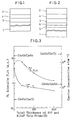
- Fig. 1 shows an example of a semiconductor device including a GaAs layer 2 grown over a Si substrate 1 by means of a MOCVD system.
- superlattice layers 3 each of which consists of gallium phosphide (GaP) with a lattice constant nearly equal to that of Si, and of gallium arsenide- phosphide (GaAsP) with a lattice constant different from that of GaP / and is about 200A (20 nm) in thickness.
- GaP gallium phosphide
- GaAsP gallium arsenide- phosphide
- superlattice layers 3 On the GaP/GaAsP superlattice layers 3 are then grown 10 superlattice layers 4 each of which consists of GaAsP and GaAs and is about 200A (20 nm) in thickness.
- the superlattice layers 3 and 4 thus grown form an intermediate layer to absorb the lattice mismatching between Si and GaAs.
- the GaAs layer 2 about 2 ⁇ m in thickness is lastly grown onto GaAsP/GaAs superlattice layers 4.
- the employed substrate 1 is made of n-type (100) silicon and trimethylgallium (Ga(CH 3 ) 3 ), trimethylaluminum (A1(CH 3 ) 3 ), arsine (AsH 3 ) and phosphine (PH 3 ) are used as the source materials of elements constituting the grown crystal layers.
- the GaAs layer 2 with a smooth top surface can be grown on the Si substrate 1 in a single growth process without any pre-cracking treatment for the V column elements by employing a horizontal atmospheric-pressure induction-heating furnace as a reactor.
- the more detailed process of the crystal growth in the above mentioned embodiment is as follows.
- the Si substrate 1 is first heated at 1000 °C in a hydrogen atmosphere for about 10 minutes in order to remove silicon dioxide (Si0 2 ) deposited on the Si substrate 1.
- 10 GaP/GaAsP superlattice layers 3 are grown at a growth temperature of 830 °C and the growth of 10 GaAsP/GaAs superlattice layers 4 follows.
- the GaAs layer 2 about 2 ⁇ m in thickness is lastly grown at 730 °C on the superlattice layers 4.
- the GaP superlattice constituent is grown from Ga(CH 3 ) 3 and PH 3
- the GaAsP superlattice constituent is grown from Ga(CH 3 ) 3 , AsH 3 and PH 3
- the GaAs layer is grown from Ga(CH 3 ) 3 and AsH 3 , all the source materials being supplied into the reactor.
- a second embodiment is explained.
- This embodiment is concerned with another process of growing the GaAs layer 2 over the Si substrate 1 made of n-type (100) Si by means of the MOCVD reactor system similarly as in the first embodiment.
- a phosphide aluminum (AlP) thin film 5 which is capable of firmly joining to and therefore easily grown on the Si substrate 1 and 100A (10 nm) in thickness and a gallium-aluminum phosphide (AlGaP) thin film 6 100A (10 nm) in thickness is formed on the film 5.
- AlP phosphide aluminum
- AlGaP gallium-aluminum phosphide
- GaP/GaAsP superlattice layers 3, each being 200A (20 nm) in thickness and 10 GaAsP/GaAs superlattice layers 4, each being 200A (20 nm) in thickness are grown in the same manner as in the first embodiment.
- the thin films 5 and 6 and the superlattice layers 3 and 4 form an intermediate layer to absorb the lattice mismatching between the Si substrate 1 and the GaAs layer 2, which is lastly grown on the intermediate layer.
- the reactor and the source materials for growing the intermediate layer and the uppermost GaAs layer 2 are the same as those employed in the first embodiment.
- the AlP thin film 5 in the intermediate layer is grown from A1(CH3)3 and PH 3 and the AlGaP thin film 6 is grown from Al(CH 3 ) 3 , Ga(CH 3 )3 and PH 3 , all the source materials being similarly supplied into the reactor.
- the superlattice layers 3 and 4 and the uppermost GaAs layer 2 are grown in the same manner as in the first embodiment.
- the total thickness of the AlP film 5 and the AlGaP thin film 6 has interrelations with the PL intensity and the carrier concentration in the uppermost GaAs layer 2.
- the PL intensity of the present growth crystal is maximum around 100A (10 nm) of the total thickness of the AlP thin film 5 and the AlGaP thin film 6 and the carrier concentration is increased by reducing the total thickness, rising acutely with the decreasing total thickness.
- the number of superlattice layers of each kind or the thickness of the intermediate layer of the second embodiment has interrelations with PL/n and n.
- PL/n is maximum about 10 superlattice layers and n increases monotonically with the increasing number of superlattice layers as shown in Fig. 4.
- Table 1 lists the full-width at half maximum (meV) * of the device of the first embodiment, i.e. GaAs/(GaAsP/GaAs)/ (GaP/GaAsP)/Si substrate, of that of the second embodiment, i.e. GaAs/(GaAsP/GaAs)/(GaP/GaAsP)/AlGaP/AlP/Si substrate, * this refers to a cure showing the PL intensity against the energy
- GaAs/Ge/Si substrate at 150 °K i.e. GaAs/Ge/Si substrate at 150 °K.
- the crystalline properties either of the device GaAs/(GaAsP/GaAs)/(GaP/ GaAsP)/Si substrate of the first embodiment or that GaAs/ (GaAsP/GaAs)/(GaP/GaAsP)/AlGaP/AlP/Si substrate of the second embodiment are superior to those of the usual device GaAs/Ge/Si substrate.
- the crystalline properties are especially improved by introducing the AlP thin film 5 and the AlGaP thin film 6 into the intermediate layer.
- the above mentioned process of growing the GaAs layer 2 over the Si substrate 1 via the intermediate layer including constituent superlattice layers can provide devices having a PL intensity higher than that of the usual devices in which the Ge intermediate layer is inserted.
- the process also makes it possible to produce cheaply a device having a PL intensity equal to that of a GaAs crystal layer grown on a GaAs substrate that is heretofore considered to be impractical because of its high production cost.
- the semiconductor device according to the present invention inexpensive and extremely efficient solar cells can be manufactured and light emitting devices which cannot be made of Si, an indirect gap semiconductor, can easily be formed on Si substrates. It is therefore possible to produce novel devices in which the light emitting devices are combined integrally with various electronic components made of Si. It is moreover possible to prepare high-speed or microwave-communication devices in the form of monolithic semiconductor elements including various integralcircuits, the freedom of manufacturing electronic devices being thereby largely extended.
- the present invention has a utility of providing an inexpensive, superior in crystalline properties and efficiently photoluminescent device by means of the process in which the intermediate layer having constituent superlattice layers is formed between the Si substrate and the GaAs single crystal layer in order to absorb the lattice mismatching between them.
Abstract
Description
- This invention relates to semiconductor devices having a gallium arsenide (GaAs) single crystal layer formed on a silicon (Si) substrate, which are necessary for producing such semiconductor structures as are employed, for example, in solar cells, microwave-communication devices and the like. The invention also relates to a method for producing such a semiconductor device.
- As a semiconductor device employed in the above mentioned devices, one is known which consists of a GaAs layer grown on a GaAs substrate (for example Journal of Crystal Growth 55 (1981) 213-222 North-Holland Publishing Company). Such a semiconductor device, however, is not practical since its production cost is high.
- It was found that when a GaAs single crystal is grown on a Si substrate, an intermediate layer of germanium (Ge) must first be formed on the Si substrate, for example by evaporation, as a kind of moderator material to absorb the mismatching effects originating from the differences between the lattice constants and between the coefficients of thermal expansion of Si and GaAs. The GaAs single crystal layer on the Si substrate is then obtained by growing a GaAs layer on the intermediate layer.
- The provision of the GaAs layer onto a Si substrate by this method, however, requires special technical steps other than the metalorganic chemical vapor deposition (MOCVD) process, as the ion cluster beam or vacuum evaporation technique. These additional steps suffer from the shortcoming that the cost of production of the GaAS layer becomes high and the performance of produced GaAS layers widely diverges owing to the variable crystalline properties governed notably by the structural condition of the formed Ge layer. It is a further shortcoming that the photoluminescence (PL) intensity of the GaAs layer provided on a Ge layer is smaller by one order of magnitude than that of an uppermost layer of a GaAS single crystal grown, for example, on a GaAs substrate.
- It is therefore a first object of the present invention to provide a semiconductor device having a GaAs single crystal layer on a Si substrate which can be produced by the MOCVD process alone.
- It is a second object of the present invention to provide such a semiconductor device which is inexpensive and in which the GaAs single crystal layer is superior in crystalline properties and efficiently photoluminescent.
- It is a third object of the present invention to provide a method of producing such a semiconductor device.
- These objects are achieved with a semiconductor device as claimed in
claim 1 and a method as claimed inclaim 4. - According to the present invention, an intermediate layer which has constituent superlattice layers intended to absorb the lattice mismatching between Si and GaAs is first formed on a Si substrate and a GaAs layer is then grown on the intermediate layer.
- Specific embodiments of the invention are characterized in the dependent claims.
- Other objects and advantages of the invention will become apparent during the following discussion of the accompanying drawings.
-
- Fig. 1 is a sectional view showing the construction of different layers of a semiconductor device as a first embodiment of the present invention;
- Fig. 2 is a view similar to Fig. 1 of a semiconductor device as a second embodiment of the present invention;
- Fig. 3 is a graph exhibiting the dependence of the measured PL intensity and carrier concentration of the device of Fig. 2 on the total thickness of AlP and AlGaP thin films; and
- Fig. 4 is a graph exhibiting the dependence of the measured PL intensity and carrier density of the device of Fig. 3 on the number of superlattice layers of one kind.
- Referring to Fig. 1, a first embodiment of the present invention is explained. Fig. 1 shows an example of a semiconductor device including a
GaAs layer 2 grown over aSi substrate 1 by means of a MOCVD system. On theSi substrate 1 are first grown 10superlattice layers 3 each of which consists of gallium phosphide (GaP) with a lattice constant nearly equal to that of Si, and of gallium arsenide- phosphide (GaAsP) with a lattice constant different from that of GaP/and is about 200A (20 nm) in thickness. On the GaP/GaAsP superlattice layers 3 are then grown 10superlattice layers 4 each of which consists of GaAsP and GaAs and is about 200A (20 nm) in thickness. Thesuperlattice layers GaAs layer 2 about 2 µm in thickness is lastly grown onto GaAsP/GaAs superlattice layers 4. The employedsubstrate 1 is made of n-type (100) silicon and trimethylgallium (Ga(CH3)3), trimethylaluminum (A1(CH3)3), arsine (AsH3) and phosphine (PH3) are used as the source materials of elements constituting the grown crystal layers. The GaAslayer 2 with a smooth top surface can be grown on theSi substrate 1 in a single growth process without any pre-cracking treatment for the V column elements by employing a horizontal atmospheric-pressure induction-heating furnace as a reactor. - The more detailed process of the crystal growth in the above mentioned embodiment is as follows. The
Si substrate 1 is first heated at 1000 °C in a hydrogen atmosphere for about 10 minutes in order to remove silicon dioxide (Si02) deposited on theSi substrate 1. Thereafter, 10 GaP/GaAsP superlattice layers 3 are grown at a growth temperature of 830 °C and the growth of 10 GaAsP/GaAs superlattice layers 4 follows. TheGaAs layer 2 about 2 µm in thickness is lastly grown at 730 °C on thesuperlattice layers 4. The GaP superlattice constituent is grown from Ga(CH3)3 and PH3, the GaAsP superlattice constituent is grown from Ga(CH3)3, AsH3 and PH3, and the GaAs layer is grown from Ga(CH3)3 and AsH3, all the source materials being supplied into the reactor. - An experiment was carried out to measure the PL intensity from the uppermost surface of the device provided by the aforementioned process in which the intermediate layer consisting of the GaP/
GaAsP superlattice layers 3 and GaAsP/GaAs superlattice layers 4 is grown on theSi substrate 1 as moderator material to absorb the lattice mismatching between theGaAs layer 2 and theSi substrate 1. It has been experimentally confirmed that the PL intensity of the device according to the present embodiment is larger by one order of magnitude than that of the uppermost surface of a usual prior art device referred to before in which a Ge intermediate layer is grown between a lower Si substrate and an upper GaAs layer. - Referring now to Fig. 2, a second embodiment is explained. This embodiment is concerned with another process of growing the
GaAs layer 2 over theSi substrate 1 made of n-type (100) Si by means of the MOCVD reactor system similarly as in the first embodiment. On theSi substrate 1 is first formed a phosphide aluminum (AlP)thin film 5 which is capable of firmly joining to and therefore easily grown on theSi substrate 1 and 100A (10 nm) in thickness and a gallium-aluminum phosphide (AlGaP) thin film 6 100A (10 nm) in thickness is formed on thefilm 5. Thereafter, 10 GaP/GaAsP superlattice layers 3, each being 200A (20 nm) in thickness and 10 GaAsP/GaAs superlattice layers 4, each being 200A (20 nm) in thickness are grown in the same manner as in the first embodiment. Thethin films 5 and 6 and thesuperlattice layers Si substrate 1 and theGaAs layer 2, which is lastly grown on the intermediate layer. The reactor and the source materials for growing the intermediate layer and theuppermost GaAs layer 2 are the same as those employed in the first embodiment. The AlPthin film 5 in the intermediate layer is grown from A1(CH3)3 and PH3 and the AlGaP thin film 6 is grown from Al(CH3)3, Ga(CH3)3 and PH3, all the source materials being similarly supplied into the reactor. Thesuperlattice layers uppermost GaAs layer 2 are grown in the same manner as in the first embodiment. - An improvement is experimentally confirmed in the surface morphology of the GaAs crystal layer provided by the present process in which the AlP
thin film 5, the AlGaP thin film 6, the GaP/GaAsP superlattice layers 3, the GaAsP/GaAs superlattice layers 4, these four forming the intermediate layer to absorb the aforementioned lattice mismatching and theGaAs layer 2, are successively grown in this order on or over theSi substrate 1. In addition, it has been confirmed by experiments that this device has a PL intensity not less than that of the device of the first embodiment. - As the result of some experiments, it has become apparent that the total thickness of the
AlP film 5 and the AlGaP thin film 6 has interrelations with the PL intensity and the carrier concentration in theuppermost GaAs layer 2. According to the results of the experiments, the PL intensity of the present growth crystal is maximum around 100A (10 nm) of the total thickness of the AlPthin film 5 and the AlGaP thin film 6 and the carrier concentration is increased by reducing the total thickness, rising acutely with the decreasing total thickness. These experimental results are exhibited in Fig. 3 where n represents the carrier number per cm3 in theGaAs layer 2, i.e. the carrier concentration and PL/n represents PL intensity per carrier concentration. - It has also been found experimentally that the number of superlattice layers of each kind or the thickness of the intermediate layer of the second embodiment has interrelations with PL/n and n. PL/n is maximum about 10 superlattice layers and n increases monotonically with the increasing number of superlattice layers as shown in Fig. 4.
- Table 1 lists the full-width at half maximum (meV)* of the device of the first embodiment, i.e. GaAs/(GaAsP/GaAs)/ (GaP/GaAsP)/Si substrate, of that of the second embodiment, i.e. GaAs/(GaAsP/GaAs)/(GaP/GaAsP)/AlGaP/AlP/Si substrate, *this refers to a cure showing the PL intensity against the energy
- and of that according to the prior art, i.e. GaAs/Ge/Si substrate at 150 °K.

- Since a decrease of the PL full-width at half maximum (meV) indicates an improvement of the crystalline properties of the device, it is seen from Table 1 that the crystalline properties either of the device GaAs/(GaAsP/GaAs)/(GaP/ GaAsP)/Si substrate of the first embodiment or that GaAs/ (GaAsP/GaAs)/(GaP/GaAsP)/AlGaP/AlP/Si substrate of the second embodiment are superior to those of the usual device GaAs/Ge/Si substrate. The crystalline properties are especially improved by introducing the AlP
thin film 5 and the AlGaP thin film 6 into the intermediate layer. - The above mentioned process of growing the
GaAs layer 2 over theSi substrate 1 via the intermediate layer including constituent superlattice layers can provide devices having a PL intensity higher than that of the usual devices in which the Ge intermediate layer is inserted. The process also makes it possible to produce cheaply a device having a PL intensity equal to that of a GaAs crystal layer grown on a GaAs substrate that is heretofore considered to be impractical because of its high production cost. - With use of the semiconductor device according to the present invention, inexpensive and extremely efficient solar cells can be manufactured and light emitting devices which cannot be made of Si, an indirect gap semiconductor, can easily be formed on Si substrates. It is therefore possible to produce novel devices in which the light emitting devices are combined integrally with various electronic components made of Si. It is moreover possible to prepare high-speed or microwave-communication devices in the form of monolithic semiconductor elements including various integralcircuits, the freedom of manufacturing electronic devices being thereby largely extended.
- In conclusion, the present invention has a utility of providing an inexpensive, superior in crystalline properties and efficiently photoluminescent device by means of the process in which the intermediate layer having constituent superlattice layers is formed between the Si substrate and the GaAs single crystal layer in order to absorb the lattice mismatching between them.
- As many apparantely widely different embodiments of the present invention may be made without departing from the spirit and scope thereof, it is to be understood that the invention is not limited to the specific embodiments thereof except as defined in the appended claims.
Claims (4)
Applications Claiming Priority (2)
| Application Number | Priority Date | Filing Date | Title |
|---|---|---|---|
| JP213188/84 | 1984-10-09 | ||
| JP59213188A JPS6191098A (en) | 1984-10-09 | 1984-10-09 | Gallium arsenide crystal grown on silicon base and method thereof |
Publications (3)
| Publication Number | Publication Date |
|---|---|
| EP0177903A2 true EP0177903A2 (en) | 1986-04-16 |
| EP0177903A3 EP0177903A3 (en) | 1987-09-09 |
| EP0177903B1 EP0177903B1 (en) | 1991-01-16 |
Family
ID=16634992
Family Applications (1)
| Application Number | Title | Priority Date | Filing Date |
|---|---|---|---|
| EP85112542A Expired EP0177903B1 (en) | 1984-10-09 | 1985-10-03 | Semiconductor device having a gallium arsenide crystal layer grown on a silicon substrate and method for producing it |
Country Status (5)
| Country | Link |
|---|---|
| US (1) | US4789421A (en) |
| EP (1) | EP0177903B1 (en) |
| JP (1) | JPS6191098A (en) |
| CA (1) | CA1265980A (en) |
| DE (1) | DE3581353D1 (en) |
Cited By (5)
| Publication number | Priority date | Publication date | Assignee | Title |
|---|---|---|---|---|
| EP0214610A2 (en) * | 1985-09-03 | 1987-03-18 | Daido Tokushuko Kabushiki Kaisha | Epitaxial gallium arsenide semiconductor wafer and method of producing the same |
| FR2620863A1 (en) * | 1987-09-22 | 1989-03-24 | Thomson Csf | OPTOELECTRONIC DEVICE BASED ON III-V COMPOUNDS ON SILICON SUBSTRATE |
| EP0331433A1 (en) * | 1988-03-01 | 1989-09-06 | Fujitsu Limited | Semiconductor substrate comprising wafer substrate and compound semiconductor layer |
| DE3932277A1 (en) * | 1988-09-30 | 1990-04-05 | Mitsubishi Electric Corp | Micro-electronic semiconductor device with lattice adaptation - by superlattice for contact area between them and with alternative material removed where devices are made in one of materials |
| EP0450228A2 (en) * | 1990-03-30 | 1991-10-09 | Mitsubishi Denki Kabushiki Kaisha | Semiconductor device formed on a silicon substrate or a silicon layer and methods of making the same |
Families Citing this family (9)
| Publication number | Priority date | Publication date | Assignee | Title |
|---|---|---|---|---|
| US5578521A (en) * | 1986-11-20 | 1996-11-26 | Nippondenso Co., Ltd. | Semiconductor device with vaporphase grown epitaxial |
| JPH01107515A (en) * | 1987-10-20 | 1989-04-25 | Daido Steel Co Ltd | Manufacture of semiconductor element |
| US5194395A (en) * | 1988-07-28 | 1993-03-16 | Fujitsu Limited | Method of producing a substrate having semiconductor-on-insulator structure with gettering sites |
| JPH0237771A (en) * | 1988-07-28 | 1990-02-07 | Fujitsu Ltd | Soi substrate |
| US5198269A (en) * | 1989-04-24 | 1993-03-30 | Battelle Memorial Institute | Process for making sol-gel deposited ferroelectric thin films insensitive to their substrates |
| JP3111644B2 (en) * | 1992-06-09 | 2000-11-27 | 三菱化学株式会社 | Gallium arsenide arsenide epitaxial wafer |
| US5993981A (en) * | 1997-04-18 | 1999-11-30 | Raytheon Company | Broadband protective optical window coating |
| US20070252216A1 (en) * | 2006-04-28 | 2007-11-01 | Infineon Technologies Ag | Semiconductor device and a method of manufacturing such a semiconductor device |
| NO20093193A1 (en) * | 2009-10-22 | 2011-04-26 | Integrated Solar As | Process for the preparation of photoelectric solar cells and a multifunctional solar cell |
Family Cites Families (6)
| Publication number | Priority date | Publication date | Assignee | Title |
|---|---|---|---|---|
| FR2225207B1 (en) * | 1973-04-16 | 1978-04-21 | Ibm | |
| US4066481A (en) * | 1974-11-11 | 1978-01-03 | Rockwell International Corporation | Metalorganic chemical vapor deposition of IVA-IVA compounds and composite |
| US4517047A (en) * | 1981-01-23 | 1985-05-14 | The United States Of America As Represented By The Secretary Of The Army | MBE growth technique for matching superlattices grown on GaAs substrates |
| US4578127A (en) * | 1982-08-13 | 1986-03-25 | At&T Bell Laboratories | Method of making an improved group III-V semiconductor device utilizing a getter-smoothing layer |
| JPS6012724A (en) * | 1983-07-01 | 1985-01-23 | Agency Of Ind Science & Technol | Growing method of compound semiconductor |
| US4588451A (en) * | 1984-04-27 | 1986-05-13 | Advanced Energy Fund Limited Partnership | Metal organic chemical vapor deposition of 111-v compounds on silicon |
-
1984
- 1984-10-09 JP JP59213188A patent/JPS6191098A/en active Granted
-
1985
- 1985-09-27 US US06/780,910 patent/US4789421A/en not_active Expired - Fee Related
- 1985-10-01 CA CA000491985A patent/CA1265980A/en not_active Expired - Fee Related
- 1985-10-03 DE DE8585112542T patent/DE3581353D1/en not_active Expired - Fee Related
- 1985-10-03 EP EP85112542A patent/EP0177903B1/en not_active Expired
Non-Patent Citations (3)
| Title |
|---|
| APPLIED PHYSICS LETTERS, vol. 43, no. 8, 15th October 1983, pages 759-761, American Institute of Physics, New York, US; R.M. BIEFELD et al.: "Independently variable band gaps and lattice constants in GaAsP strained-layer superlattices" * |
| ELECTRONICS LETTERS, vol. 20, no. 22, 25th October 1984, page 916-918, Hitchin Herts, GB; T. SOGA et al.: "MOCVD growth of GaAs on Si substrates with AlGaP and strained superlattice layers" * |
| JAPANESE JOURNAL OF APPLIED PHYSICS. SUPPLEMENTS 16th INTERNATIONAL CONFERENCE SOLID STATE DEVICES AND MATERIALS, 30th August - 1st September 1984, Kobe, JP, pages 115-119, Tokyo, JP; J.C.C. FAN: "Monolithic integration of GaAs and Si" * |
Cited By (11)
| Publication number | Priority date | Publication date | Assignee | Title |
|---|---|---|---|---|
| EP0214610A2 (en) * | 1985-09-03 | 1987-03-18 | Daido Tokushuko Kabushiki Kaisha | Epitaxial gallium arsenide semiconductor wafer and method of producing the same |
| EP0214610A3 (en) * | 1985-09-03 | 1987-12-02 | Daido Tokushuko Kabushiki Kaisha | Epitaxial gallium arsenide semiconductor wafer and method of producing the same |
| US4928154A (en) * | 1985-09-03 | 1990-05-22 | Daido Tokushuko Kabushiki Kaisha | Epitaxial gallium arsenide semiconductor on silicon substrate with gallium phosphide and superlattice intermediate layers |
| FR2620863A1 (en) * | 1987-09-22 | 1989-03-24 | Thomson Csf | OPTOELECTRONIC DEVICE BASED ON III-V COMPOUNDS ON SILICON SUBSTRATE |
| EP0309333A1 (en) * | 1987-09-22 | 1989-03-29 | Thomson-Csf | Optoelectronic device formed by III-V-compounds on a silicon substrate |
| US4897699A (en) * | 1987-09-22 | 1990-01-30 | Thomson-Csf | Group III-V compound based optoelectronic device on silicon substrate |
| EP0331433A1 (en) * | 1988-03-01 | 1989-09-06 | Fujitsu Limited | Semiconductor substrate comprising wafer substrate and compound semiconductor layer |
| DE3932277A1 (en) * | 1988-09-30 | 1990-04-05 | Mitsubishi Electric Corp | Micro-electronic semiconductor device with lattice adaptation - by superlattice for contact area between them and with alternative material removed where devices are made in one of materials |
| EP0450228A2 (en) * | 1990-03-30 | 1991-10-09 | Mitsubishi Denki Kabushiki Kaisha | Semiconductor device formed on a silicon substrate or a silicon layer and methods of making the same |
| EP0450228A3 (en) * | 1990-03-30 | 1991-11-27 | Mitsubishi Denki Kabushiki Kaisha | Semiconductor device formed on a silicon substrate or a silicon layer |
| US5136347A (en) * | 1990-03-30 | 1992-08-04 | Mitsubishi Denki Kabushiki Kaisha | Semiconductor structure |
Also Published As
| Publication number | Publication date |
|---|---|
| EP0177903B1 (en) | 1991-01-16 |
| US4789421A (en) | 1988-12-06 |
| EP0177903A3 (en) | 1987-09-09 |
| JPH0463039B2 (en) | 1992-10-08 |
| JPS6191098A (en) | 1986-05-09 |
| DE3581353D1 (en) | 1991-02-21 |
| CA1265980A (en) | 1990-02-20 |
Similar Documents
| Publication | Publication Date | Title |
|---|---|---|
| Soga et al. | Characterization of epitaxially grown GaAs on Si substrates with III‐V compounds intermediate layers by metalorganic chemical vapor deposition | |
| US5019529A (en) | Heteroepitaxial growth method | |
| US7323764B2 (en) | Buffer structure for modifying a silicon substrate | |
| EP0177903A2 (en) | Semiconductor device having a gallium arsenide crystal layer grown on a silicon substrate and method for producing it | |
| JPH0812844B2 (en) | (III) -Group V compound semiconductor and method for forming the same | |
| EP0291346B1 (en) | A laminated structure of compound semiconductors | |
| JPH04504031A (en) | Substrate processing and method for manufacturing semiconductor devices using the substrate | |
| US5492860A (en) | Method for growing compound semiconductor layers | |
| Hashimoto et al. | Initial growth stage of GaN on Si substrate by alternating source supply using dimethyl-hydrazine | |
| JP2000150388A (en) | Iii nitride semiconductor thin film and manufacture thereof | |
| Soga et al. | Nucleation mechanisms for compound semiconductors grown on Si by MOCVD | |
| US5341006A (en) | Semiconductor device having diffusion-preventing layer between III-V layer and IV layer | |
| JPH01120011A (en) | Inp semiconductor thin film | |
| KR20150035413A (en) | Epitaxial growth of compound semiconductors using lattice-tuned domain-matching epitaxy | |
| JPH0214513A (en) | Formation of compound semiconductor layer | |
| JP3124616B2 (en) | Method for growing compound semiconductor thin film | |
| Karam et al. | Growth and Characterization of InP/GaAs on SOI by MOCVD | |
| JPH01723A (en) | 3-Group V compound crystal article and method for forming the same | |
| JPS6258614A (en) | Arsenide galium epitaxial wafer and manufacture thereof | |
| JPH0633224B2 (en) | Method for epitaxial growth of compound semiconductor on heterogeneous substrate | |
| JPH057359B2 (en) | ||
| JPH05234907A (en) | Gaas substrate and its manufacture | |
| JPH0582964B2 (en) | ||
| etsuo Soga et al. | Characterization of epitaxJaUy grown GaAs on 5i substrates with~ nv compounds intermediate layers by meta. forganic chemical vapor deposition | |
| JPH0496320A (en) | Method of growing thin film semiconductor crystal |
Legal Events
| Date | Code | Title | Description |
|---|---|---|---|
| PUAI | Public reference made under article 153(3) epc to a published international application that has entered the european phase |
Free format text: ORIGINAL CODE: 0009012 |
|
| AK | Designated contracting states |
Kind code of ref document: A2 Designated state(s): DE FR GB NL |
|
| 17P | Request for examination filed |
Effective date: 19860912 |
|
| PUAL | Search report despatched |
Free format text: ORIGINAL CODE: 0009013 |
|
| AK | Designated contracting states |
Kind code of ref document: A3 Designated state(s): DE FR GB NL |
|
| 17Q | First examination report despatched |
Effective date: 19890601 |
|
| GRAA | (expected) grant |
Free format text: ORIGINAL CODE: 0009210 |
|
| AK | Designated contracting states |
Kind code of ref document: B1 Designated state(s): DE FR GB NL |
|
| REF | Corresponds to: |
Ref document number: 3581353 Country of ref document: DE Date of ref document: 19910221 |
|
| ET | Fr: translation filed | ||
| PLBE | No opposition filed within time limit |
Free format text: ORIGINAL CODE: 0009261 |
|
| STAA | Information on the status of an ep patent application or granted ep patent |
Free format text: STATUS: NO OPPOSITION FILED WITHIN TIME LIMIT |
|
| 26N | No opposition filed | ||
| PGFP | Annual fee paid to national office [announced via postgrant information from national office to epo] |
Ref country code: GB Payment date: 19960924 Year of fee payment: 12 |
|
| PGFP | Annual fee paid to national office [announced via postgrant information from national office to epo] |
Ref country code: FR Payment date: 19961009 Year of fee payment: 12 |
|
| PGFP | Annual fee paid to national office [announced via postgrant information from national office to epo] |
Ref country code: DE Payment date: 19961011 Year of fee payment: 12 |
|
| PGFP | Annual fee paid to national office [announced via postgrant information from national office to epo] |
Ref country code: NL Payment date: 19961029 Year of fee payment: 12 |
|
| PG25 | Lapsed in a contracting state [announced via postgrant information from national office to epo] |
Ref country code: GB Free format text: LAPSE BECAUSE OF NON-PAYMENT OF DUE FEES Effective date: 19971003 |
|
| PG25 | Lapsed in a contracting state [announced via postgrant information from national office to epo] |
Ref country code: FR Free format text: THE PATENT HAS BEEN ANNULLED BY A DECISION OF A NATIONAL AUTHORITY Effective date: 19971031 |
|
| PG25 | Lapsed in a contracting state [announced via postgrant information from national office to epo] |
Ref country code: NL Free format text: LAPSE BECAUSE OF NON-PAYMENT OF DUE FEES Effective date: 19980501 |
|
| GBPC | Gb: european patent ceased through non-payment of renewal fee |
Effective date: 19971003 |
|
| NLV4 | Nl: lapsed or anulled due to non-payment of the annual fee |
Effective date: 19980501 |
|
| PG25 | Lapsed in a contracting state [announced via postgrant information from national office to epo] |
Ref country code: DE Free format text: LAPSE BECAUSE OF NON-PAYMENT OF DUE FEES Effective date: 19980701 |
|
| REG | Reference to a national code |
Ref country code: FR Ref legal event code: ST |