EP0058417A2 - Method for transmitting time-division multiplexed data - Google Patents
Method for transmitting time-division multiplexed data Download PDFInfo
- Publication number
- EP0058417A2 EP0058417A2 EP82101070A EP82101070A EP0058417A2 EP 0058417 A2 EP0058417 A2 EP 0058417A2 EP 82101070 A EP82101070 A EP 82101070A EP 82101070 A EP82101070 A EP 82101070A EP 0058417 A2 EP0058417 A2 EP 0058417A2
- Authority
- EP
- European Patent Office
- Prior art keywords
- bit
- error
- data
- code
- bits
- Prior art date
- Legal status (The legal status is an assumption and is not a legal conclusion. Google has not performed a legal analysis and makes no representation as to the accuracy of the status listed.)
- Granted
Links
- 238000000034 method Methods 0.000 title claims abstract description 37
- 238000012937 correction Methods 0.000 claims description 53
- 238000001514 detection method Methods 0.000 claims description 22
- 239000011159 matrix material Substances 0.000 claims description 11
- 125000004122 cyclic group Chemical group 0.000 claims description 3
- 208000011580 syndromic disease Diseases 0.000 description 17
- 238000010586 diagram Methods 0.000 description 12
- 230000005236 sound signal Effects 0.000 description 9
- 230000005540 biological transmission Effects 0.000 description 4
- 230000001360 synchronised effect Effects 0.000 description 4
- 238000010276 construction Methods 0.000 description 3
- 230000015556 catabolic process Effects 0.000 description 1
- 238000004891 communication Methods 0.000 description 1
- 238000007796 conventional method Methods 0.000 description 1
- 230000007423 decrease Effects 0.000 description 1
- 230000003247 decreasing effect Effects 0.000 description 1
- 238000006731 degradation reaction Methods 0.000 description 1
- 238000012986 modification Methods 0.000 description 1
- 230000004048 modification Effects 0.000 description 1
- 230000010363 phase shift Effects 0.000 description 1
- 238000012545 processing Methods 0.000 description 1
- 230000004044 response Effects 0.000 description 1
Images


Classifications
-
- H—ELECTRICITY
- H04—ELECTRIC COMMUNICATION TECHNIQUE
- H04L—TRANSMISSION OF DIGITAL INFORMATION, e.g. TELEGRAPHIC COMMUNICATION
- H04L1/00—Arrangements for detecting or preventing errors in the information received
- H04L1/004—Arrangements for detecting or preventing errors in the information received by using forward error control
- H04L1/0056—Systems characterized by the type of code used
- H04L1/0057—Block codes
-
- H—ELECTRICITY
- H04—ELECTRIC COMMUNICATION TECHNIQUE
- H04H—BROADCAST COMMUNICATION
- H04H40/00—Arrangements specially adapted for receiving broadcast information
- H04H40/18—Arrangements characterised by circuits or components specially adapted for receiving
- H04H40/27—Arrangements characterised by circuits or components specially adapted for receiving specially adapted for broadcast systems covered by groups H04H20/53 - H04H20/95
- H04H40/36—Arrangements characterised by circuits or components specially adapted for receiving specially adapted for broadcast systems covered by groups H04H20/53 - H04H20/95 specially adapted for stereophonic broadcast receiving
- H04H40/45—Arrangements characterised by circuits or components specially adapted for receiving specially adapted for broadcast systems covered by groups H04H20/53 - H04H20/95 specially adapted for stereophonic broadcast receiving for FM stereophonic broadcast systems receiving
-
- H—ELECTRICITY
- H04—ELECTRIC COMMUNICATION TECHNIQUE
- H04L—TRANSMISSION OF DIGITAL INFORMATION, e.g. TELEGRAPHIC COMMUNICATION
- H04L1/00—Arrangements for detecting or preventing errors in the information received
- H04L1/004—Arrangements for detecting or preventing errors in the information received by using forward error control
- H04L1/0041—Arrangements at the transmitter end
-
- H—ELECTRICITY
- H04—ELECTRIC COMMUNICATION TECHNIQUE
- H04L—TRANSMISSION OF DIGITAL INFORMATION, e.g. TELEGRAPHIC COMMUNICATION
- H04L1/00—Arrangements for detecting or preventing errors in the information received
- H04L1/004—Arrangements for detecting or preventing errors in the information received by using forward error control
- H04L1/0045—Arrangements at the receiver end
Definitions
- an electrical wave is transmitted from a broadcasting station on the earth to an artificial satellite in which it is received, amplified and frequency-converted thereby transmitted to a listener or receiver on the earth again.
- the audio broadcasting requires a band width narrower than that of the television broadcasting. If one broadcasting channel assigned to the television broadcasting is used for the audio broadcasting, it can make the audio broadcasting with much more plurality of channels multiplexed. In this case, a time-sharing multiplex can be utilized. More particularly, an information digital signal achieved by PCM (Pulse Code Modulation)-modulating an audio signal is time-sharing multiplexed in order to perform the audio broadcasting with high quality.
- PCM Pulse Code Modulation
- an object of the present invention is to provide a novel method for transmitting time-sharing multidata which can solve the afore-described problems.
- Another object of the present invention is to provide a method for transmitting time-sharing multidata which can error-correct the received data of the desired channel .
- usin g a bit rate sufficiently lower than that upon transmitting.
- another object of the present invention is to provide a method for transmitting time-sharing multidata which can produce a receiving apparatus or receiver for receiving a transmitted data series at a low cost.
- Another object of the present invention is to provide a method for transmitting time-sharing multidata in which even when a bit number of the redundant bits for synchronization is less, it is possible to secure the bit number necessary for a frame synchronizing signal.
- another object of the present invention is to provide a method for transmitting time-sharing multidata which is free from a problem of a transmission of an error when input noises exceeding an error correction capability are caused and which is effective for use in the PCM broadcasting in high quality.
- another object of the present invention is to provide a method for transmitting time-sharing multidata which can-reduce both error-correction ratio and interpolation ⁇ error particularly when the redundancy of the error correction code is small.
- a method for transmitting time-sharing multidata in which data series of a plurality of channels are time-sharing multiplexed to form a transmitting data series having the steps of adding an error detecting or error correcting redundant bit and a synchronizing redundant bit to an information bit of a predetermined number contained in the respective data series of said channels to form one transmitting unit, forming bit groups in a manner as to take each bit as one group which is corresponding to each other between the channels with respect to the information bit, the error detecting or error correcting redundant bit and the synchronizing redundant bit of said one transmitting unit of each of said channels, time-sharing multiplexing the data series so as to form one frame in which these bit groups are sequentially continued to each other and using a bit pattern of the bit groups-in the synchronizing redundant bit as a frame synchronizing signal of the transmitting data series.
- a channel for transmitting a television signal and a channel for transmitting an audio signal are modulated by a single carrier wave and then transmitted as a microwave of, for example, about 14 GH z through a transmitting antenna l A .
- This micro wave is received by a geostationary satellite 2 once and after being amplified, it is frequency-converted to a micro wave with a frequency of, for example, about 12 GH Z and transmitted again to the earth.
- the micro wave received by an antenna 3A is demodulated by a TV (television) tuner 4 so as to be reproduced by a television receiver 5.
- the audio signal is demodulated by a program selector 6 and then reproduced by, for example, a Hi-Fi (high fidelity) apparatus 7.
- the audio signal transmitted from the broadcasting station 1 is such signal that stereophonic audio data of twelve transmitting channels are time-sharing multiplexed.
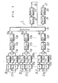
- Fig. 3 shows an arrangement of the broadcasting station, namely, the transmitting side in which right and left stereophonic audio signals each of the broadcasting channels of first to twelfth channels (hereinafter, simply referred to as CHl to CH12) are respectively supplied to input terminals 8L a , 8R a , 8L b , 8R b ⁇ 8L l , BR l .
- PCM data series are respectively supplied to error correction encoders 12 , 12 b , ⁇ 12l whereby they arc encoded for error-correction in each channel.
- error-correction codes are used block codes in which for example, a BCH code and a parity code are combined as will be described later.
- the respective output data series from the error-correction encoders 12a, 12 b ⁇ 12 l are fed to synchronizing signal adding circuits 13a, 13 b ⁇ 13 l thereby added with block synchronizing signals.
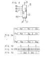
- F ig. 4 illustrates a data format of a subblock SB i common to the respective channels of the signals appearing at the respective intermediate output terminals 14a, 14 b ⁇ 14 so as to be supplied to the multiplexer 15.
- One subblock SB i is formed of total 48 bits composing data bits dL 0 to dL 13 of 14bits for the left channel, data bits dR 0 to dR 13 of 14 bits for the right channel, service bits s 0 and s 1 of 2 bits, error-correcting redundant bits c 0 to c 14 of 15 bits and synchronizing redundant bits f 0 , f 1 and f 2 of 3 bits.
- the one frame is constructed such that a bit group dL 0 , dL 1 ⁇ dL 13 of the left channel data, a bit group dR 0 , dR 1 ⁇ dR 13 of the right channel data, service bit groups s 0 and s 1 , error-correcting redundant bit groups c 0 to c 14 and synchronizing bit groups f 0 , f 1 and f 2 are arranged in sequence.
- Each bit group is formed of 12 bits and it is a set of a plurality of bits corresponding to each other between the channels from Clll to CHl2.
- bit group dL 0 is the set from the MSB dL 01 of the data in the left channel in CHl to the respective MSBs dL 02 , dL 03 ⁇ ⁇ ⁇ dL 012 of CH2, CH3 ⁇ ⁇ ⁇ CHl2.
- a load pulse seen in Fig. 7B is produced in a timing nearly central of the bit cell, so that the MSBs, for example, from CHI to CH12 are loaded to the shift register 22 one at a time at its falling.
- the data bits are taken out at the output terminal 25 of the shift register 22 by the clock pulse C K having a period of 1/12 of bit period of the data. Therefore, the output data series become such one that the bit groups dL O , dL, are sequentially connected to one other as shown in Fig. 7D.
- the data series time-sharing multiplexed as described above is supplied from the multiplexer 15 to a PSK (Phase Shift Keying) modulating circuit or modulator 16.
- a PSK (Phase Shift Keying) modulating circuit or modulator 16 In this embodiment, a four-phase P SK modulation is utilized in the PSK modulator 16 in which a carrier of 113 MH z is modulated by a transmitting data with a transmitting rate of 18.432 Mb/sec.
- the four-phase PSK modulation is to phase-modulate the data series such that the phase of the carrier is made different by each in accordance with the bit pattern (four ways may be possible as 00, 01, 10 and 11) of 2 bits with respect to the data bit.
- the output from the PSK modulator 16 is supplied to and frequency-converted to a signal with a carrier frequency of about 14 GH Z by frequency converters 17 and 19.
- Reference numeral 18 denotes a microwave transmitting line such as a coaxial cable connected between the frequency converters 17 and 19.
- the output signal derived from the frequency converter 19 is fed to and amplified by a microwave amplifier 20 whereby it is produced at an output terminal 21 and hence transmitted from the transmitting antenna l A (refer to Fig. 1).
- the artificial satellite 2 receives and amplify s this transmitted signal thereby permitting it to be frequency-converted to a signal with a carrier frequency of about 12 GH Z and then transmitted to a number of receivers on the earth.
- F ig. 8 schematically shows a construction of the receiving apparatus 6 provided at each listener or receiving station 3 (refer to Fig. 1) in which the received signal thrc the receiving antenna 3A (in Fig. 1) is supplied to an input terminal 26 and then delivered hy way of a microwave amplifie 27, a frequency converter 28 and a coaxial cable 29 to a frequency converter 30 so as to be recovered to the signal having the carrier frequency of 113 MH Z and PSK-converted.
- This signal is delivered to and demodulated by a P SK demodulator 31.
- the carrier used in such demodulation is formed of the received signal employing a PLL (Phase Locked Loop) circuit.
- PLL Phase Locked Loop
- the demodulated output derived from the PSK demodulator 31 is fed to a synchronous separating circuit or separator 32 and then delivered to a channel selector 33 whereby only the data series of a desired channel from CHl to CH12 is selected.
- the received data series of the specif broadcasting channel selected from the channel selector 33 i supplied to an error correcting and error-concealing circuit 34.
- This received data series have the same data format as that in the transmitting side as shown in Fig. 4 and is corrected for error in each one subblock. In this case, when the detected error is beyond the error-correcting capability of the code, the error-concealment is performed to conceal the error.
- the error-corrected or error-conceal signal is delivered from the error-correcting and error-concealing circuit 34 to a D/A converter 35 so as to be returned to the audio signal, then it is separated into the right and left channels of the stereo by an analog switch 36 and then supplied through low pass filters 37L and 37R to audio output terminals 38L and 38R.
- These separated stereophonic audio signals are supplied through an amplifier of the Hi-Fi apparatus 7 (Fig. 2) to two speakers so that the listener can reproduce them in the stereophonic mode.
- the channel selector 33 can be achieved by using a shift register 39 and a latch circuit 40 as illustrated in Fig. 9.
- the received data series is supplied to an input terminal 41 of the shift register 39 and then taken thereinto by a clock pulse supplied thereto through a terminal 42.
- the shift register 39 is of 12-bit type and in a certain timing, stores 12 bits of dL 01 to dL 012 contained in the bit group dL O .
- the output of 12 bits from this shift register 39 are supplied to the latch circuit 40, wherein each bit group consisting of the bits corresponding to one another from CH1 to CH12 as mentioned above is taken into the latch circuit 40 by a latch pulse supplied thereto through a terminal 43.
- the latch pulse has a bit period at the stages before the signals from the respective broadcasting channels are time-sharing multiplexed and owing to this latch pulse, the output of 12 bits from the latch circuit 40 are introduced into twelve input terminals of a selector 44.
- the selector 44 serves to set a connecting position of the channel in response to the broadcasting station which the listener desires to receive.
- Fig. 9 indicates a case where the channel CH2 is selected and therefore the received data series of CH2 is produced at an output terminal 45 of this selector 44.
- the code error occurs as a form of a random error. It is important that the code error is corrected and cancealed with good efficiency in the PCM broadcasting in high quality. Thus, if the error-correction and error-concealment capability is strengthened, it is expected that a degradation of a C/N (Carrier to Noise) ratio in the received signal may be improved and a service area may be widened.
- C/N Carrier to Noise
- a convolutional code is widely employed mainly in view of easy decoding. But, in the presence of the input noise beyond the error-correction capability, the convolutional code inherits a problem that the error is transmitted to the following code due to the input noise and hence the convolu- tional code is not suitable for the PCM broadcasting in high quality.
- the error-correcting code the present invention employs, it is preferred that some words are prepared to comprise ore block and the error-correcting code is generated based on such block unit.
- Parity Q 0 to Q13 of double error correcting BCH code (42 bits or 30 bits) each consisting of 12 bits of q 0 to q 11 are added to each of the row directions. Also, at the end of the column direction corresponding to the data D 0 to D 13 is added a vertical parity P D consisting of 30 bits formed of n 0 to P 29 .
- a vertical parity P Q comprised of 12 bits formed of p 30 to p 41 relative to the parity Q 0 to Q13 of the BCH code is formed likewise. This vertical parity P Q is made coincident with the parity Q 14 of the BCH code relative to the vertical parity P D .
- the parity Q i of the BCH code if an encode matrix is taken as H E , is expressed as follows:
- the vertical parity P Q corresponding to the parity Q. in the BCH code is expressed as follows:
- the vertical parity P Q corresponding to the parity Q. in the BCH code is expressed as follows:
- the data to which the error pointers are added are interpolated.
- the method for interpolating the data such one is proposed that the mean value located before and after the correct data in the original time series is used as the interpolation data.
- this SEC-DED code is used to correct 1 bit code error and to detect 2 bits code error.
- the error -detecting pointer is added to this SEC-DED code to thereby detect the erroneous correction and so forth and if necessary, to perform the interpolation therefor.
- C R CC cyclic redundancy check code
- the interpolation error becomes greater if the block unit is made larger.
- the encoding method will be described first.
- the error-correcting encoders 12a to 12 l (hereinafter, represented generally as 12) at the transmitting in station 1 in Fig. 3 are provided to encode the respective inputted data series as illustrated in Fig. 11.
- the number of the block, the bit length of one block and so on are different from those of the previous example in Fig. 10.
- the service bit is omitted.
- the PCM data W i comprising these respective subblocks SB' i is interleaved in odd- and -even -numbered manner. That is, odd-numbered PCM data W 0 , W 2 , ⁇ W 14 compose one block and even-numbered PCM data W 1 , W 3 , ⁇ , W 15 compose another block.
- the CRCC of 16 bits generated from each block forms the block pointer in each block. Then, on the basis of this CRCC, it can be detected whether or not the code error exists in each block.
- This CRCC of 16 bits is assigned to P' 0 and P' 1 of each subblock SB' i 2 bits by
- the check bits q' 0 , q' 1 ⁇ , q' 6 are added to the PCM data W' i formed of the data bit of 28 bits length and the CRCC of 2 bits length to thereby SEC-DED encode the same.
- the encoder 12 can be constructed as, for example, shown in Fig. 12.
- a RAM (Random Access Memory) 45 is provided to perform a block interleave.
- the PCM data W 0 to W 15 transferred from the adder 11 including the adders lla to 11l ( F ig. 3) through a terminal 46 to the encoder 12 are written in this RAM 45 and thereafter, the PCM data W 0 , W 2 , ⁇ ⁇ ⁇ ,W 14 , W 1 , W 3 , ⁇ ⁇ ⁇ , W 15 are sequentially read out therefrom.
- the data series formed as described above is supplied to a check bit generating circuit or generator 54 wherein the check bit of 7 bits length and the synchronizing bit of 1 bit length are added to each subblock SB' i .
- the data series from the OR circuit 53 is fed to a shift register 55 as a serial input. While the serial output from this shift register 55 is delivered to an OR circuit 56, the output of 1 bit is, at the same time, supplied from the input side of the shift register 55 to one of each of input terminals of 7 AND circuits 57.
- data responsive to the parity generating matrix HE was already written in a ROM (Read Only Memory) 58. This data is supplied to and serial-to-parallel-converted sequentiallyi n 7 bits each by a shift register 59, and then it is supplied through a latch circuit 60 to the other input terminals of the AND circuits 57.
- the AND circuits 57 are employed to form the check bits in association with 7 exclusive OR circuits 61 and seven D flip-flops 62.
- the parity generating matrix HE is taken as the check bits responsive to the data bits based upon the parity generating matrix HE are generated.
- the check bits thus achieved are supplied to and parallel-to-serial-converted at a shift register 63 and then supplied to the OR circuit 56.
- the check bits of 7 bits length are added to the left channel data bit of 14 bits length, the right channel data bit of same 14 bits length and the CRCC bit of 2 bits length, which are then delivered through a terminal 64 to the synchronizing adding circuit 13 including the circuits 13a to 13 t located at the later stages (refer to Fig. 3) whereby they are added with the synchronizing bits of 1 bit length to comprise the code word V of 38 bits length.
- the error correcting and error concealing circuit or the decoder 34 in Fig. 8 can be constructed as, for example, seen in Fig. 13.
- the 1 bit error detecting output E 1 is also applied to the AND circuits 75 wherein the output "1" is supplied to either of the adders 69 responsive to the erroneous position to correct the error in case of 1 bit code error.
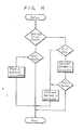
- the CRCC bit of 2 bits is supplied to a CRCC decoder 77 together with the error detecting output E 0 , the 1 bit error detecting output E l and the 2 bits error detecting output E 2 .
- the CRCC decoder 77 is operated as illustrated in F ig. 14 for its output to control the transmitting interpolation circuit 77. More specifically, when there are neither of the 1 bit code error correction nor the 2 bits code error detection and the block pointer based upon the CRCC (no error in block unit exists), the decoded data is transferred as it is. In this case, since the block pointer based upon the CRCC is not raised, a probability is quite high that the errorless or correct transmission of data is performed.
- the subblock where the error code correction is carried out is interpolated.
- 3 bits code error or-the like but not 1 bit code error is caused in fact and such code error is erroneously corrected since the decoding circuit 65 is mainly aimed for the S E C-DED code.
- Such erroneous correction can be avoided by interpolating the captioned subblock..
- the subblock correcponding thereto is interpolated alone,-the interpolation error is reduced greatly.
- the subblock where 2 bits code error is detected is interpolated. In this case, since the error detection is positively.or reliably carried out and only the corresponding subblock is interpolated, the interpolation error is less.
- 1 bit code error is corrected in each subblock by employing the SEC-DED code and also 2 bits code error is interpolated. Thereafter, the code error of the block unit is detected by the CRCC. Then, such a case where there is an error in 1 bit code error correction and the code error more than 3 bits which can not be detected can be detected in the block unit.
- 2 9 bits code error detection appears and so on can be acquired, only the subblock responsive thereto is interpolated.
- the redundancy degree becomes quite small.
- the block interleave is performed so that it is possible to cope with the burst error.
- each bit corresponding to one other between the channels is grouped as one group to form the bit groups and the data series are time-sharing multiplexed in such a manner as to form one frame where these bit groups are sequentially connected, in the receiving side, the error on the received data on the desired channel can be corrected with the bit rate sufficiently lower than that upon the transmission. Therefore, the receiving apparatus can be realized at a low cost.
- bit pattern in the bit group of the synchronizing redundant bit is used as the frame synchronizing signal of the transmitting data series, even if the bit number of the synchronizing redundant bit is less, it is possible to secure the bit number necessary for the frame synchronizing signal.
- the data format of the codeword is such one that the data is block-interleaved as shown in Fig. 11, it can be easily understood that the block interleave may not be applied thereto. But, instead, it is also be possible that 16 subblocks of the PCM data W 0 to W 15 might comprise one block and the CRCC bit might be assigned bit by bit to each subblock. In such case, the redundancy degree of the CRCC bit becomes one-half so that the service bit (1 bit length) can be added thereto by the remaining one-half amount.
- the entire block is interpolated.
- all the blocks are interpolated to prevent the data with the erroneous code from being transmitted while it is not interpolated. If all the blocks are interpolated, ' it is naturally considered that the interpolation error becomes large. But, such case is very rare so that the interpolation error can be reduced on the whole.
- each bit responsive to one another between the channels is grouped into one group to form a bit group and the data is time-sharing multiplexed in such manner as to form one frame where bit group is connected in sequence, in the receiving side, the received data of the desired channel can be error-corrected with the bit rate sufficiently lower than that upon the transmission. Consequently, the receiving apparatus can be produced at a low cost.
- bit pattern of the bit group composing the synchronizing redundant bit is employed as the frame synchronizing signal of the transmitting data series, even if the bit number of the synchronizing redundant bit is less, the bit number required for the frame synchronizing signal can be secured.
- the data format of the data series to be supplied to the multiplexer 15 in Fig. 3 which is used to time-sharing multiplex the data series is not limited to that in Fig. 2. But instead, if such format is made the same in all the transmitting channels, any given one may be used.
Abstract
Description
- The present invention relates generally to a method for transmitting time-sharing multidata and is directed mo. particularly to a method for transmitting time-sharing multidata suitable for use with a satellite broadcasting.
- With a satellite broadcasting system, an electrical wave is transmitted from a broadcasting station on the earth to an artificial satellite in which it is received, amplified and frequency-converted thereby transmitted to a listener or receiver on the earth again. Today, any one of television and audio broadcastings can be made in association with the satellite broadcasting. The audio broadcasting requires a band width narrower than that of the television broadcasting. If one broadcasting channel assigned to the television broadcasting is used for the audio broadcasting, it can make the audio broadcasting with much more plurality of channels multiplexed. In this case, a time-sharing multiplex can be utilized. More particularly, an information digital signal achieved by PCM (Pulse Code Modulation)-modulating an audio signal is time-sharing multiplexed in order to perform the audio broadcasting with high quality.
- As a method for time-sharing multiplexing a plurality of data, such a conventional method is proposed that a pre-determined time is divided by the number of the channels, time positions are assigned to the corresponding divided channels
each and data from the respective channels are time-base compressed and inserted to the time positions thereby permitting a redundant code for detecting an error or for correcting the error and a redundant code for synchronization to be added to the multiplexed data. This time-sharing multiplexing method is used when a plurality of the broadcasting stations on the earth perform both the transmitting and receiving of the radio waves. But, in the case where the transmitting side-and the receiving side are distinguished obviously from each other like the satellite broadcasting, the time-sharing multiplexing method as set forth above will not be suitable for the satellite broadcasting in view of the fact that the apparatus owned by the listener becomes complicated in construction. - Therefore, an object of the present invention is to provide a novel method for transmitting time-sharing multidata which can solve the afore-described problems.
- Especially, another object of the present invention is to provide a method for transmitting time-sharing multidat, wherein upon receiving a transmitted data series, it is sufficient to use a receiving apparatus or receiver which can be actuated by a clock with low frequency.
- Further, another object of the present invention is to provide a method for transmitting time-sharing multidata which can error-correct the received data of the desired channel.using a bit rate sufficiently lower than that upon transmitting.
- Still further, another object of the present invention is to provide a method for transmitting time-sharing multidata which can produce a receiving apparatus or receiver for receiving a transmitted data series at a low cost.
- Still further, another object of the present invention is to provide a method for transmitting time-sharing multidata in which even when a bit number of the redundant bits for synchronization is less, it is possible to secure the bit number necessary for a frame synchronizing signal.
- Still further, another object of the present invention is to provide a method for transmitting time-sharing multidata which is free from a problem of a transmission of an error when input noises exceeding an error correction capability are caused and which is effective for use in the PCM broadcasting in high quality.
- Still further, another object of the present invention is to provide a method for transmitting time-sharing multidata which can-reduce both error-correction ratio and interpolation}error particularly when the redundancy of the error correction code is small.
- According to an aspect of the present invention, there is provided a method for transmitting time-sharing multidata in which data series of a plurality of channels are time-sharing multiplexed to form a transmitting data series having the steps of adding an error detecting or error correcting redundant bit and a synchronizing redundant bit to an information bit of a predetermined number contained in the respective data series of said channels to form one transmitting unit, forming bit groups in a manner as to take each bit as one group which is corresponding to each other between the channels with respect to the information bit, the error detecting or error correcting redundant bit and the synchronizing redundant bit of said one transmitting unit of each of said channels, time-sharing multiplexing the data series so as to form one frame in which these bit groups are sequentially continued to each other and using a bit pattern of the bit groups-in the synchronizing redundant bit as a frame synchronizing signal of the transmitting data series.
- The other objects, features and advantages of the present invention will become apparent from the following description taken in conjunction with the accompanying drawings through which the like references designate the same elements and parts.
-
- Fig. 1 is a schematic diagram showing a satellite broadcasting system to which the present invention can be applied;
- Fig. 2 is a schematic diagram showing a receiving system of a satellite broadcasting system shown in Fig. 1, particularly a receiving system installed within a general listener's home;
- Fig. 3 is a schematic block diagram showing one embodiment of the present invention provided at a transmitting side;
- Figs. 4 and 5 are schematic diagrams showing data formats of one embodiment according to the present invention;
- Fig. 6 is a block diagram showing one example of a multiplexer for use in time-sharing multiplexing data;
- Figs. 7A to 7D are respectively timing charts used to explain the operations of the multiplexer in Fig. 6;
- Fig. 8 is a block diagram schematically showing a construction of one embodiment of the present invention provided at a receiving side;
- Fig. 9 is a schematic block diagram of one example of a channel selector;
- Fig. 10 is a schematic diagram. showing an error correction block format of an error correction method used in the present invention;
- Fig. 11 is a schematic diagram showing an error correction block format of another error correction method in the present invention;
- Fig. 12 is a block'diagram schematically showing an encoder which generates the error correction block seen in Fig. 11;
- Fig. 13 is a block diagram schematically showing a decoder corresponding to the encoder in Fig. 12; and
- Fig. 14 is a diagram partially showing a flow chart of the decoder in Fig. 13.
- One embodiment of the present invention applied to a satellite broadcasting will be described hereinafter.
- As shown in Fig. 1, in a
broadcasting station 1 on the earth, a channel for transmitting a television signal and a channel for transmitting an audio signal are modulated by a single carrier wave and then transmitted as a microwave of, for example, about 14 GHz through a transmitting antenna lA. This micro wave is received by ageostationary satellite 2 once and after being amplified, it is frequency-converted to a micro wave with a frequency of, for example, about 12 GHZ and transmitted again to the earth. - As shown in Fig. 2, in a
receiving station 3 on the earth, the micro wave received by anantenna 3A is demodulated by a TV (television)tuner 4 so as to be reproduced by atelevision receiver 5. At the same time, the audio signal is demodulated by aprogram selector 6 and then reproduced by, for example, a Hi-Fi (high fidelity)apparatus 7. The audio signal transmitted from thebroadcasting station 1 is such signal that stereophonic audio data of twelve transmitting channels are time-sharing multiplexed. - Fig. 3 shows an arrangement of the broadcasting station, namely, the transmitting side in which right and left stereophonic audio signals each of the broadcasting channels of first to twelfth channels (hereinafter, simply referred to as CHl to CH12) are respectively supplied to input terminals 8La, 8Ra, 8Lb, 8Rb ··· 8Lℓ, BRℓ. These right and Peft stereophonic audio signals are fed channel by channel through low pass filters 9La, 9Ra, 9Lb, 9Rb ··· 9Lℓ, 9Rℓ to D/A (Digital to Analog)
converters - These PCM data series are respectively supplied to
error correction encoders correction encoders 12a, 12b ··· 12ℓ are fed to synchronizingsignal adding circuits 13a, 13b ··· 13ℓ thereby added with block synchronizing signals. - In this way, the signals in which error-correcting redundant bits and synchronizing redundant bits are added with at every channel of CH1 to CH12 appear at
intermediate output terminals multiplexer 15 whereby they are time-sharing multiplexed. - Fig. 4 illustrates a data format of a subblock SBi common to the respective channels of the signals appearing at the respective
intermediate output terminals multiplexer 15. One subblock SBi is formed of total 48 bits composing data bits dL0 to dL13 of 14bits for the left channel, data bits dR0 to dR13 of 14 bits for the right channel, service bits s0 and s1 of 2 bits, error-correcting redundant bits c0 to c14 of 15 bits and synchronizing redundant bits f0, f1 and f2 of 3 bits. The service bits s0 and s1 are spare bits utilized to add a necessary information in case of identification or discrimination and control and so forth. The right and left audio data dL0 to dL13 and dR0 to dR13 are so formed that they are placed in a sequential order form MSB (Most Significant Bit) of dL0' dR0 to LSB (Least Significant Bit) of dL13, dR13. - The data series of the respective broadcasting channels having the data format as shown in Fig. 4 are synchronized with each other and delivered to the
multiplexer 15, by which they are time-sharing multiplexed bit by bit taking one subblock SBi as a unit. The total of 12 subblocks SBi contained in the respective broadcasting channels from CHl to CH12 construct one frame of the transmitted data series as shown in Fig. 5. - The one frame is constructed such that a bit group dL0, dL1 ··· dL13 of the left channel data, a bit group dR0, dR1 ··· dR13 of the right channel data, service bit groups s0 and s1, error-correcting redundant bit groups c0 to c14 and synchronizing bit groups f0, f1 and f2 are arranged in sequence. Each bit group is formed of 12 bits and it is a set of a plurality of bits corresponding to each other between the channels from Clll to CHl2. For example, the bit group dL0 is the set from the MSB dL01 of the data in the left channel in CHl to the respective MSBs dL02, dL03 · · · dL012 of CH2, CH3 · · · CHl2.
- The
multiplexer 15 for time-sharing multiplexing the data series as described above can be realized by ashift register 22 as shown in Fig. 6. In other words, the data series of the broadcasting channels from CH1 to CH12 are supplied to 12 parallel input terminals o.f theshift register 22, namely, theintermediate output terminals 14a to 14ℓ, by which they are taken bit by bit in theshift register 22 in accordance with a load pulse applied to its terminal 23 and then produced at aserial output terminal 25 by a clock pulse CK supplied thereto through a terminal 24. - Assuming that data bits of the channels from CH1 to CH12 synchronized one other as shown in Fig. 7A are supplied to the
parallel input terminals 14a to 14i of theshift register 22, a load pulse seen in Fig. 7B is produced in a timing nearly central of the bit cell, so that the MSBs, for example, from CHI to CH12 are loaded to theshift register 22 one at a time at its falling. Then, as shown in Fig. 7C, the data bits are taken out at theoutput terminal 25 of theshift register 22 by the clock pulse CK having a period of 1/12 of bit period of the data. Therefore, the output data series become such one that the bit groups dLO, dL, are sequentially connected to one other as shown in Fig. 7D. - Turning back to Fig. 3, the data series time-sharing multiplexed as described above is supplied from the
multiplexer 15 to a PSK (Phase Shift Keying) modulating circuit ormodulator 16. In this embodiment, a four-phase PSK modulation is utilized in thePSK modulator 16 in which a carrier of 113 MHz is modulated by a transmitting data with a transmitting rate of 18.432 Mb/sec. The four-phase PSK modulation is to phase-modulate the data series such that the phase of the carrier is made different by each
PSK modulator 16 is supplied to and frequency-converted to a signal with a carrier frequency of about 14 GHZ byfrequency converters Reference numeral 18 denotes a microwave transmitting line such as a coaxial cable connected between thefrequency converters frequency converter 19 is fed to and amplified by amicrowave amplifier 20 whereby it is produced at anoutput terminal 21 and hence transmitted from the transmitting antenna lA (refer to Fig. 1). - The
artificial satellite 2 receives and amplifys this transmitted signal thereby permitting it to be frequency-converted to a signal with a carrier frequency of about 12 GHZ and then transmitted to a number of receivers on the earth. - Fig. 8 schematically shows a construction of the receiving
apparatus 6 provided at each listener or receiving station 3 (refer to Fig. 1) in which the received signal thrc the receivingantenna 3A (in Fig. 1) is supplied to aninput terminal 26 and then delivered hy way of amicrowave amplifie 27, afrequency converter 28 and acoaxial cable 29 to afrequency converter 30 so as to be recovered to the signal having the carrier frequency of 113 MHZ and PSK-converted. This signal is delivered to and demodulated by a PSK demodulator 31. The carrier used in such demodulation is formed of the received signal employing a PLL (Phase Locked Loop) circuit. The demodulated output derived from the PSK demodulator 31 is fed to a synchronous separating circuit or separator 32 and then delivered to achannel selector 33 whereby only the data series of a desired channel from CHl to CH12 is selected. The received data series of the specif broadcasting channel selected from the channel selector 33 i supplied to an error correcting and error-concealingcircuit 34. This received data series have the same data format as that in the transmitting side as shown in Fig. 4 and is corrected for error in each one subblock. In this case, when the detected error is beyond the error-correcting capability of the code, the error-concealment is performed to conceal the error. The error-corrected or error-conceal signal is delivered from the error-correcting and error-concealingcircuit 34 to a D/A converter 35 so as to be returned to the audio signal, then it is separated into the right and left channels of the stereo by ananalog switch 36 and then supplied throughlow pass filters audio output terminals 38L and 38R. These separated stereophonic audio signals are supplied through an amplifier of the Hi-Fi apparatus 7 (Fig. 2) to two speakers so that the listener can reproduce them in the stereophonic mode. - To perform various data processings at the receiving side as mentioned above, are used the frame synchronizing signals f0, f1 and f2 which were separated by the synchronous separating circuit 32.
- The
channel selector 33 can be achieved by using a shift register 39 and alatch circuit 40 as illustrated in Fig. 9. In detail, the received data series is supplied to aninput terminal 41 of the shift register 39 and then taken thereinto by a clock pulse supplied thereto through a terminal 42. The shift register 39 is of 12-bit type and in a certain timing,stores 12 bits of dL01 to dL012 contained in the bit group dLO. The output of 12 bits from this shift register 39 are supplied to thelatch circuit 40, wherein each bit group consisting of the bits corresponding to one another from CH1 to CH12 as mentioned above is taken into thelatch circuit 40 by a latch pulse supplied thereto through a terminal 43. The latch pulse has a bit period at the stages before the signals from the respective broadcasting channels are time-sharing multiplexed and owing to this latch pulse, the output of 12 bits from thelatch circuit 40 are introduced into twelve input terminals of aselector 44. Theselector 44 serves to set a connecting position of the channel in response to the broadcasting station which the listener desires to receive. Fig. 9 indicates a case where the channel CH2 is selected and therefore the received data series of CH2 is produced at anoutput terminal 45 of thisselector 44. - In the PCM broadcasting using the broadcasting satellite and so on as described above, the code error occurs as a form of a random error. It is important that the code error is corrected and cancealed with good efficiency in the PCM broadcasting in high quality. Thus, if the error-correction and error-concealment capability is strengthened, it is expected that a degradation of a C/N (Carrier to Noise) ratio in the received signal may be improved and a service area may be widened.
- In a conventional communication circuit, a convolutional code is widely employed mainly in view of easy decoding. But, in the presence of the input noise beyond the error-correction capability, the convolutional code inherits a problem that the error is transmitted to the following code due to the input noise and hence the convolu- tional code is not suitable for the PCM broadcasting in high quality.
- To avoid this, as the error-correcting code the present invention employs, it is preferred that some words are prepared to comprise ore block and the error-correcting code is generated based on such block unit.
- A practical example of the error-detecting and correcting code according to the present invention will be described hereinafter. The error-detecting and -correcting code is comprised as shown in Fig. 10. In this example, PCM data Wi of total 28 bits consisting of stereophonic audio signals of the right and left channels each formed of 14 bits per one sample at every one channel and service bit of 2 bits will form an information data Di of totally 30 bits. This information data Di is arranged in the row direction. 14' data of this information data Di are arranged as D0 to D13 in the column direction to form a matrix 30 x 14. Parity Q0 to Q13 of double error correcting BCH code (42 bits or 30 bits) each consisting of 12 bits of q0 to q11 are added to each of the row directions. Also, at the end of the column direction corresponding to the data D0 to D13 is added a vertical parity PD consisting of 30 bits formed of n0 to P29. A vertical parity PQ comprised of 12 bits formed of p30 to p41 relative to the parity Q0 to Q13 of the BCH code is formed likewise. This vertical parity PQ is made coincident with the parity Q14 of the BCH code relative to the vertical parity PD. In other words, the parity Qi of the BCH code, if an encode matrix is taken as HE, is expressed as follows:


- When the BCH code Qi and the vertical parity codes PD and PQ thus generated are transmitted by the aforesaid transmitting system, the error-correcting redundant bits c0 to c11 in the error-correcting redundant bits c0 to c14 (shown in Fig. 4) are assigned to the BCH code Qi and the remaining 3 bits from c12 to c14 are sequentially assigned to 42 bits from P0 to P41 consisting the vertical parity codes PD and PQ covering the area of 42 bits which are comprised of 14 blocks totally.
- Next, one example of the method for decoding the codes with the arrangement as set forth above will be described hereinafter.
- At first, the error-detection and -correction for the code in the row direction is performed using the parity in the BCH code. In this case, a parity check matrix HD utilizes the following one.


- The error-detection and -correction based upon the vertical parity will be carried out next.
- The error detection and error correction are performed by using syndromes SP1 and SP2 which are obtained from the following calculations


- When Spl = SP2 = 0, it is regarded that no error exists, irrespective of the presence or absence of the error pointer.
- When the error syndrome SP1 or SP2 is not zero and. when there is one error pointer, the correct data is obtained by using the error syndrome SP1 and then the correct data is used instead of the data in which the error pointer is added thereto.
- When the error syndrome SP1 or SP2 is not zero and when there are error pointers more than two, the data to which the error pointers are added are interpolated. As the method for interpolating the data, such one is proposed that the mean value located before and after the correct data in the original time series is used as the interpolation data.
- When the error pointer is zero although the error syndrome SP1 or SP2 is not zero, all the data from D0 to D13 are interpolated considering that the error detection based upon the BCH code is missed.
- According to this method, as described above, since the vertical parity check including the parity of the BCH code is performed and when the error syndrcme based upon the vertical parity check is 0, it is regarded that no error exists. In the other cases, since the error correction or the interpolation is carried out, it is possible to prevent the erroneous correction the error detection from being missed due to the BCH code.
- As another error-correcting method which can be employed in the present invention, for example, an SEC-DED (Single Error Correcting-Double Error Detecting) code may be considered.
- As its name reveal the property thereof, this SEC-DED code is used to correct 1 bit code error and to detect 2 bits code error.
- But, the SEC-DED code alone can not cope with the code error more than 3 bits, which may probably give rise to the erroneous correction.
- Therefore, such method is proposed that the error -detecting pointer is added to this SEC-DED code to thereby detect the erroneous correction and so forth and if necessary, to perform the interpolation therefor. In this case, owing to the necessity that the redundancy of the code has to be made small, it is requested that a cyclic redundancy check code (hereinafter, simply referred to as CRCC), which will form an error detecting pointer, is dispersed into each subblock (each word) to detect the error in a block unit. The larger this block becomes, the less the redundancy of the code decreases.
- However, when the erroneous correction or the like is detected by the detecting pointer so as to perform the interpolation. the interpolation error becomes greater if the block unit is made larger.
- To cope with the above aspect, in accordance with the error-correcting method which will be described in detail hereinafter, while the redundancy of the error correcting and detecting code is made small, the error correcting ratio and the interpolation error can be suppressed as small.
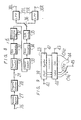
- The encoding method will be described first. The error-correcting encoders 12a to 12ℓ (hereinafter, represented generally as 12) at the transmitting in
station 1 in Fig. 3 are provided to encode the respective inputted data series as illustrated in Fig. 11. In this case, the number of the block, the bit length of one block and so on are different from those of the previous example in Fig. 10. - In other words, a subblock SB'i (i = 0, 1, 2,···, 15) is corresponding to the subblock SBi shown in Fig. 4 and consists of PCM data Wi formed of data bits dLO to dL13 of 14 bits length in the left channel and data bits dRO to dR13 of 14 bits length in the right channel, CRCC bits P'0 and P'1 of 2 bits length, detecting bits q'0 to q'6 of 7 bits length and synchronizing bit f'0 of 1 bit length to make 38 bits totally. In this case, the service bit is omitted. The PCM data Wi comprising these respective subblocks SB'i is interleaved in odd- and -even -numbered manner. That is, odd-numbered PCM data W 0, W 2, ··· W 14 compose one block and even-numbered PCM data W 1, W 3, ···, W 15 compose another block. In this case, the CRCC of 16 bits generated from each block forms the block pointer in each block. Then, on the basis of this CRCC, it can be detected whether or not the code error exists in each block. This CRCC of 16 bits is assigned to P'0 and P'1 of each subblock SB'i 2 bits by
- The check bits q'0, q'1 ···, q'6 are added to the PCM data W'i formed of the data bit of 28 bits length and the CRCC of 2 bits length to thereby SEC-DED encode the same.
- The
encoder 12 can be constructed as, for example, shown in Fig. 12. In Fig. 12, a RAM (Random Access Memory) 45 is provided to perform a block interleave. The PCM data W0 to W15 transferred from theadder 11 including the adders lla to 11ℓ (Fig. 3) through a terminal 46 to theencoder 12 are written in thisRAM 45 and thereafter, the PCM data W0, W2, · · · ,W14, W1, W3, · · · , W15 are sequentially read out therefrom. - On the other hand, the PCM data W0 to W15 delivered through the terminal 46 arc also supplied to CRCC generating circuits or
generators 41the one
CRCC generator 47 is used to generatehit composing the block pointer in the block formed of one add-numbered PCM data W0, W2 · · ·, W14 and the
other CRCC generator 48 is to generate the CRCC bit composing the block pointer at the block formed of the even-numbered PCM data W1, W3, ···, W15. The CRCC bits generated from theseCRCC generators shift registers gate circuits OR circuit 53 whereby the CRCC codes are added 2 bits length by 2 bits length to the PCM data W0, W2, ···, W14 derived from theRAM 45. - The data series formed as described above is supplied to a check bit generating circuit or generator 54 wherein the check bit of 7 bits length and the synchronizing bit of 1 bit length are added to each subblock SB'i. In other words, in accordance with the
check bit generator 54, the data series from theOR circuit 53 is fed to ashift register 55 as a serial input. While the serial output from thisshift register 55 is delivered to anOR circuit 56, the output of 1 bit is, at the same time, supplied from the input side of theshift register 55 to one of each of input terminals of 7 ANDcircuits 57. On the other hand, data responsive to the parity generating matrix HE was already written in a ROM (Read Only Memory) 58. This data is supplied to and serial-to-parallel-converted sequentiallyin 7bits each by ashift register 59, and then it is supplied through alatch circuit 60 to the other input terminals of the ANDcircuits 57. - In this case, the AND
circuits 57 are employed to form the check bits in association with 7 exclusive ORcircuits 61 and seven D flip-flops 62. In other words, if the parity generating matrix HE is taken as


circuits 61 and the D flip-flops 62. - The check bits thus achieved are supplied to and parallel-to-serial-converted at a
shift register 63 and then supplied to theOR circuit 56. As a result, in the respective subblocks SB'i, the check bits of 7 bits length are added to the left channel data bit of 14 bits length, the right channel data bit of same 14 bits length and the CRCC bit of 2 bits length, which are then delivered through a terminal 64 to thesynchronizing adding circuit 13 including the circuits 13a to 13t located at the later stages (refer to Fig. 3) whereby they are added with the synchronizing bits of 1 bit length to comprise the code word V of 38 bits length. - The error correcting and error concealing circuit or the
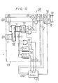
decoder 34 in Fig. 8 can be constructed as, for example, seen in Fig. 13. -
Reference numeral 65 denotes adecoding circuit 65 which will detect the erroneous correction of a code word V' (sometimes, there may be code error) transmitted through the transmitting system such as an antenna and fed to input terminal 66 and 67 of thedecoder 65 to thereby produce the data bit from output terminals 68 of thedecoder 65, thereafter. - In Fig. 13, the data of 30 bits length composing the right and left channels data bits of 14 bits lengths and the CRCC bit of 2 bits length is supplied from the
input terminal 66 to thedecoding circuit 65 of the SEC-DED code and the check bit of 7 bits length is supplied from theinpu1 terminal 67 thereto. In thisdecoding circuit 65, the PCM data Wi and the CRCC bits p'0 and p'1 are applied toadders 69. The respective data bits of 14 bits each are also supplied to asyndrome generating circuit 70. Thesyndrome generating circuit 70 is also supplied with the check bits q'0 to q'6 of 7 bits length. In this case, thesyndrome generating circuit 70 is used to perform the calculation of HD · (V')T = ST to generate a syndrome S where HD is as follows:

syndrome decoder 71 carries out such discrimination and produces the output "1" at its position responsive to the erroneous position. - The syndrome S generated at the
syndrome generating circuit 70 is supplied to anOR circuit 72, an 1 bit error detecting circuit ordetector 73 and a 2 bits error detecting circuit ordetector 74. The ORcircuit 72 is adapted to produce an error detecting output E0 and the 1 bit and 2bits error detectors - The 1 bit error detecting output E1 is also applied to the AND circuits 75 wherein the output "1" is supplied to either of the
adders 69 responsive to the erroneous position to correct the error in case of 1 bit code error. - As described above, according to the SEC-DED code, one bit error code can be corrected and two bits code error can be detected. The decoding circuit 65.produces the right and left channels data of 28 bits properly corrected and the CRCC bit of 2 bits length and of which, the right and left channels data of 28 bits are supplied to a transmitting
interpolation circuit 76. - On the other hand, the CRCC bit of 2 bits is supplied to a
CRCC decoder 77 together with the error detecting output E0, the 1 bit error detecting output El and the 2 bits error detecting output E2. In this case, theCRCC decoder 77 is operated as illustrated in Fig. 14 for its output to control the transmittinginterpolation circuit 77. More specifically, when there are neither of the 1 bit code error correction nor the 2 bits code error detection and the block pointer based upon the CRCC (no error in block unit exists), the decoded data is transferred as it is. In this case, since the block pointer based upon the CRCC is not raised, a probability is quite high that the errorless or correct transmission of data is performed. - When 1 bit code error correction is carried out once or a plurality of times and when the block pointer is not raised, the decoded data is transferred as it is. In this case, since the block pointer is not raised, it is an extremely high probability that the error correction performed in the
decoding circuit 65 is accurate. In other words, the error correction ratio is less. - When there is one or plurality of bit code errors and when the block pointer is raised, the subblock where the error code correction is carried out is interpolated. In this case, 3 bits code error or-the like but not 1 bit code error is caused in fact and such code error is erroneously corrected since the
decoding circuit 65 is mainly aimed for the SEC-DED code. Such erroneous correction can be avoided by interpolating the captioned subblock.. In addition, since the subblock correcponding thereto is interpolated alone,-the interpolation error is reduced greatly. - When 1 bit-code error correction exists once or a plurality of times and 2 bits code error detection exists once or a plurality of times and also the block pointer is raised, the subblock where the error is corrected and detected is interpolated. In this case, since it is not apparent whether or not 1 bit code correction is correct, not only the subblock where 2 bits code error is detected but also the subblock where l'bit code error correction exists are interpolated. Accordingly, the erroneous correction will never occur. In addition, the subblock responsive thereto alone is interpolated, so that there is little interpolation error in this case.
- When 2 bits code error is detected once or a plurality of times and when the block pointer is raised, the subblock where 2 bits code error is detected is interpolated. In this case, since the error detection is positively.or reliably carried out and only the corresponding subblock is interpolated, the interpolation error is less.
- Further, when neither 1 bit code error is corrected nor 2 bits code error is detected but when the block pointer is raised, all the blocks are interpolated. In this case, since it is unclear which subblock has the code error, the entire block is interpolated. If so, it is needless to say that the interpolation error is urged to become large. But, owing to the small probability that such case will occur, it can be said that the interpolation error is small as a whole.
- In accordance with the arrangement thus discussed, fundamentally speaking, 1 bit code error is corrected in each subblock by employing the SEC-DED code and also 2 bits code error is interpolated. Thereafter, the code error of the block unit is detected by the CRCC. Then, such a case where there is an error in 1 bit code error correction and the code error more than 3 bits which can not be detected can be detected in the block unit. In addition, when the information of the position where 1 bit code error correction exists, 2 9 bits code error detection appears and so on can be acquired, only the subblock responsive thereto is interpolated. On the other hand, in the case that the information of the position where the code error exists can not be obtained, all the blocks are interpolated to exclude the code error at the sacrifice of the fact that the interpolation error becomes more or less becomes large. Therefore, the interpolation error becomes small as possible and the error correction ratio becomes also small.
- Further, since as the redundant bit, the CRCC bit is dispersed 2 bits by 2 bits in each subblock to be added thereto, the redundancy degree becomes quite small.
- Also, in this example of the present invention, the block interleave is performed so that it is possible to cope with the burst error. Further, in accordance with this example, since each bit corresponding to one other between the channels is grouped as one group to form the bit groups and the data series are time-sharing multiplexed in such a manner as to form one frame where these bit groups are sequentially connected, in the receiving side, the error on the received data on the desired channel can be corrected with the bit rate sufficiently lower than that upon the transmission. Therefore, the receiving apparatus can be realized at a low cost.
- Also, since the bit pattern in the bit group of the synchronizing redundant bit is used as the frame synchronizing signal of the transmitting data series, even if the bit number of the synchronizing redundant bit is less, it is possible to secure the bit number necessary for the frame synchronizing signal.
- While in the aforesaid embodiment, the data format of the codeword is such one that the data is block-interleaved as shown in Fig. 11, it can be easily understood that the block interleave may not be applied thereto. But, instead, it is also be possible that 16 subblocks of the PCM data W0 to W15 might comprise one block and the CRCC bit might be assigned bit by bit to each subblock. In such case, the redundancy degree of the CRCC bit becomes one-half so that the service bit (1 bit length) can be added thereto by the remaining one-half amount.
- As described above, according to this decoding apparatus, after the error correction and detection of the respective subblocks are carried out based upon the check bits, the errors are detected in the block unit based on the CRCC after the error correction and detection. Accordingly, if the erroneous correction exists within the block, such erroneous correction can be positively or reliably detected based upon-the CRCC. Thus, if the interpolation is performed based upon such detection, the erroneous correction ratio is greatly reduced. In addition, since the CRCC is dispersed into the respective subblocks, the redundancy degree of the code can be made small extremely.
- Further, in accordance with the decoding apparatus of this example, when the error correction and detection exist in any one of the subblocks and at the same time, the error is detected in the block unit, the subblock where the error was corrected and detected is interpolated. Thus, the interpolation error is decreased greatly as compared with the previous case where all the blocks are interpolated. In addition, since the subblock in which the error is corrected and detected is interpolated, if the erroneous correction is carried out, such erroneous correction can be solved by the interpolation.
- Also, since the erroneous detections in the block unit are caused almost all by the erroneous code within the subblock where the error is corrected and detected, such a probability is quite low that the error detection will be caused by the erroneous code which is missed from the error correction and detection. Therefore, if so, it will hardly occur that the data containing the erroneous code may be transmitted without being interpolated.
- On the other hand, when no error is corrected and detected at any of all the subblocks but the error is detected in the block unit, the entire block is interpolated. In this case, since it can not be discriminated which of the subblock has the code error, all the blocks are interpolated to prevent the data with the erroneous code from being transmitted while it is not interpolated. If all the blocks are interpolated,' it is naturally considered that the interpolation error becomes large. But, such case is very rare so that the interpolation error can be reduced on the whole.
- As it is understood from the description of the embodiments mentioned above, according to the method for transmitting time-sharing multidata of the present invention, since the error detecting or error correcting redundant bit is added to every transmitting channel, each bit responsive to one another between the channels is grouped into one group to form a bit group and the data is time-sharing multiplexed in such manner as to form one frame where bit group is connected in sequence, in the receiving side, the received data of the desired channel can be error-corrected with the bit rate sufficiently lower than that upon the transmission. Consequently, the receiving apparatus can be produced at a low cost.
- Also, since the bit pattern of the bit group composing the synchronizing redundant bit is employed as the frame synchronizing signal of the transmitting data series, even if the bit number of the synchronizing redundant bit is less, the bit number required for the frame synchronizing signal can be secured.
- In this case, the data format of the data series to be supplied to the
multiplexer 15 in Fig. 3 which is used to time-sharing multiplex the data series is not limited to that in Fig. 2. But instead, if such format is made the same in all the transmitting channels, any given one may be used. - The above description is given on preferred embodiments of the present invention, but-it will be apparent that many modifications and variations could be effected by one skilled in the art without departing from the spirits or scope of the novel concepts of the invention, so that the scope of the invention should be determined by the appended claims only.
Claims (6)
Priority Applications (1)
| Application Number | Priority Date | Filing Date | Title |
|---|---|---|---|
| AT82101070T ATE21310T1 (en) | 1981-02-17 | 1982-02-12 | METHOD OF TRANSMISSION OF TIME-DIVISION DATA. |
Applications Claiming Priority (2)
| Application Number | Priority Date | Filing Date | Title |
|---|---|---|---|
| JP56022000A JPS57136833A (en) | 1981-02-17 | 1981-02-17 | Time-division multiplex data transmitting method |
| JP22000/81 | 1981-02-17 |
Publications (3)
| Publication Number | Publication Date |
|---|---|
| EP0058417A2 true EP0058417A2 (en) | 1982-08-25 |
| EP0058417A3 EP0058417A3 (en) | 1982-09-22 |
| EP0058417B1 EP0058417B1 (en) | 1986-08-06 |
Family
ID=12070737
Family Applications (1)
| Application Number | Title | Priority Date | Filing Date |
|---|---|---|---|
| EP82101070A Expired EP0058417B1 (en) | 1981-02-17 | 1982-02-12 | Method for transmitting time-division multiplexed data |
Country Status (6)
| Country | Link |
|---|---|
| US (1) | US4491943A (en) |
| EP (1) | EP0058417B1 (en) |
| JP (1) | JPS57136833A (en) |
| AT (1) | ATE21310T1 (en) |
| CA (1) | CA1183620A (en) |
| DE (1) | DE3272409D1 (en) |
Cited By (6)
| Publication number | Priority date | Publication date | Assignee | Title |
|---|---|---|---|---|
| EP0141431A2 (en) * | 1983-11-09 | 1985-05-15 | Sony Corporation | Digital signal transmitting and/or receiving system |
| EP0144801A2 (en) * | 1983-11-09 | 1985-06-19 | Sony Corporation | Digital signal transmitting system |
| FR2565443A1 (en) * | 1984-05-29 | 1985-12-06 | Cit Alcatel | METHODS OF DIFFUSION AND RECEPTION OF HIGH QUALITY SOUND PROGRAMS AND RECEPTION DEVICE. |
| EP0167849A2 (en) * | 1984-07-07 | 1986-01-15 | TELEFUNKEN Fernseh und Rundfunk GmbH | Digital signal transmission system, especially for satellite broadcasting |
| EP0212261A1 (en) * | 1985-08-20 | 1987-03-04 | ANT Nachrichtentechnik GmbH | Broad-band distribution and communication system |
| EP0634840A1 (en) * | 1993-07-16 | 1995-01-18 | AT&T Corp. | Unequal error protection for combined information signals |
Families Citing this family (41)
| Publication number | Priority date | Publication date | Assignee | Title |
|---|---|---|---|---|
| JPS61182342A (en) * | 1985-02-07 | 1986-08-15 | Matsushita Electric Ind Co Ltd | Data transmitter |
| JPH01245470A (en) * | 1988-03-28 | 1989-09-29 | Toshiba Corp | Rotary head type magnetic recording and reproducing device |
| CA1323456C (en) * | 1989-09-11 | 1993-10-19 | Douglas James Millar | Transmission error protection for tdma digital channels |
| US5315583A (en) * | 1991-04-11 | 1994-05-24 | Usa Digital Radio | Method and apparatus for digital audio broadcasting and reception |
| EP0537382A1 (en) * | 1991-10-15 | 1993-04-21 | ALCATEL BELL Naamloze Vennootschap | Packet transfer control arrangement and related method |
| US5642437A (en) * | 1992-02-22 | 1997-06-24 | Texas Instruments Incorporated | System decoder circuit with temporary bit storage and method of operation |
| US5313454A (en) * | 1992-04-01 | 1994-05-17 | Stratacom, Inc. | Congestion control for cell networks |
| KR950002672B1 (en) * | 1992-04-11 | 1995-03-24 | 삼성전자주식회사 | Voice data interpolation circuit |
| US5729556A (en) * | 1993-02-22 | 1998-03-17 | Texas Instruments | System decoder circuit with temporary bit storage and method of operation |
| CA2131674A1 (en) * | 1993-09-10 | 1995-03-11 | Kalyan Ganesan | High performance error control coding in channel encoders and decoders |
| KR100251641B1 (en) * | 1996-05-13 | 2000-04-15 | 김영환 | Circuit for arranging channels |
| JP3922819B2 (en) * | 1998-09-21 | 2007-05-30 | 富士通株式会社 | Error correction method and apparatus |
| US6304992B1 (en) * | 1998-09-24 | 2001-10-16 | Sun Microsystems, Inc. | Technique for correcting single-bit errors in caches with sub-block parity bits |
| US6760772B2 (en) * | 2000-12-15 | 2004-07-06 | Qualcomm, Inc. | Generating and implementing a communication protocol and interface for high data rate signal transfer |
| US7631242B2 (en) * | 2001-06-22 | 2009-12-08 | Broadcom Corporation | System, method and computer program product for mitigating burst noise in a communications system |
| US8812706B1 (en) | 2001-09-06 | 2014-08-19 | Qualcomm Incorporated | Method and apparatus for compensating for mismatched delays in signals of a mobile display interface (MDDI) system |
| US7007220B2 (en) * | 2002-03-01 | 2006-02-28 | Broadlogic Network Technologies, Inc. | Error correction coding across multiple channels in content distribution systems |
| BRPI0410885B1 (en) * | 2003-06-02 | 2018-01-30 | Qualcomm Incorporated | GENERATE AND IMPLEMENT A SIGNAL AND INTERFACE PROTOCOL FOR HIGHER DATA RATES |
| AU2004300958A1 (en) * | 2003-08-13 | 2005-02-24 | Qualcomm, Incorporated | A signal interface for higher data rates |
| ATE424685T1 (en) * | 2003-09-10 | 2009-03-15 | Qualcomm Inc | INTERFACE FOR HIGH DATA RATE |
| CN1894931A (en) * | 2003-10-15 | 2007-01-10 | 高通股份有限公司 | High data rate interface |
| EP1692842A1 (en) | 2003-10-29 | 2006-08-23 | Qualcomm Incorporated | High data rate interface |
| TWI381686B (en) * | 2003-11-12 | 2013-01-01 | Qualcomm Inc | High data rate interface with improved link control |
| BRPI0416895A (en) * | 2003-11-25 | 2007-03-06 | Qualcomm Inc | High data rate interface with enhanced link synchronization |
| CA2731265A1 (en) * | 2003-12-08 | 2005-06-23 | Qualcomm Incorporated | High data rate interface with improved link synchronization |
| EP1733537A1 (en) * | 2004-03-10 | 2006-12-20 | Qualcomm, Incorporated | High data rate interface apparatus and method |
| WO2005091593A1 (en) * | 2004-03-17 | 2005-09-29 | Qualcomm Incorporated | High data rate interface apparatus and method |
| BRPI0509147A (en) * | 2004-03-24 | 2007-09-11 | Qualcomm Inc | High data rate interface equipment and method |
| US8650304B2 (en) * | 2004-06-04 | 2014-02-11 | Qualcomm Incorporated | Determining a pre skew and post skew calibration data rate in a mobile display digital interface (MDDI) communication system |
| KR100914420B1 (en) * | 2004-06-04 | 2009-08-27 | 퀄컴 인코포레이티드 | High data rate interface apparatus and method |
| US8699330B2 (en) | 2004-11-24 | 2014-04-15 | Qualcomm Incorporated | Systems and methods for digital data transmission rate control |
| US8873584B2 (en) | 2004-11-24 | 2014-10-28 | Qualcomm Incorporated | Digital data interface device |
| US20060161691A1 (en) * | 2004-11-24 | 2006-07-20 | Behnam Katibian | Methods and systems for synchronous execution of commands across a communication link |
| US8723705B2 (en) * | 2004-11-24 | 2014-05-13 | Qualcomm Incorporated | Low output skew double data rate serial encoder |
| US8539119B2 (en) * | 2004-11-24 | 2013-09-17 | Qualcomm Incorporated | Methods and apparatus for exchanging messages having a digital data interface device message format |
| US8692838B2 (en) * | 2004-11-24 | 2014-04-08 | Qualcomm Incorporated | Methods and systems for updating a buffer |
| US8667363B2 (en) * | 2004-11-24 | 2014-03-04 | Qualcomm Incorporated | Systems and methods for implementing cyclic redundancy checks |
| US7412642B2 (en) * | 2005-03-09 | 2008-08-12 | Sun Microsystems, Inc. | System and method for tolerating communication lane failures |
| FR2891422B1 (en) * | 2005-09-23 | 2007-11-30 | Alcatel Sa | SATELLITE RADIO AND TERRESTRIAL SYNCHRONIZED TRANSMISSION OF DATA GROUP SUBGROUMS FOR RADIO COMMUNICATION TERMINALS |
| US8730069B2 (en) * | 2005-11-23 | 2014-05-20 | Qualcomm Incorporated | Double data rate serial encoder |
| US8692839B2 (en) * | 2005-11-23 | 2014-04-08 | Qualcomm Incorporated | Methods and systems for updating a buffer |
Citations (2)
| Publication number | Priority date | Publication date | Assignee | Title |
|---|---|---|---|---|
| GB1578469A (en) * | 1977-11-05 | 1980-11-05 | Marconi Co Ltd | Tropospheric scatter radio communications systems |
| US4237553A (en) * | 1978-12-26 | 1980-12-02 | Bell Telephone Laboratories, Incorporated | Data packet multiplexing in a staggered fashion |
Family Cites Families (12)
| Publication number | Priority date | Publication date | Assignee | Title |
|---|---|---|---|---|
| US3622984A (en) * | 1969-11-05 | 1971-11-23 | Ibm | Error correcting system and method |
| JPS5361211A (en) * | 1976-11-13 | 1978-06-01 | Fujitsu Ltd | Multiplication device |
| US4161719A (en) * | 1977-10-04 | 1979-07-17 | Ncr Corporation | System for controlling synchronization in a digital communication system |
| JPS54128605A (en) * | 1978-03-30 | 1979-10-05 | Toshiba Corp | Additional system of error check bit |
| JPS5556744A (en) * | 1978-10-23 | 1980-04-25 | Sony Corp | Pcm signal transmission device |
| US4211997A (en) * | 1978-11-03 | 1980-07-08 | Ampex Corporation | Method and apparatus employing an improved format for recording and reproducing digital audio |
| IT7921131A0 (en) * | 1979-03-20 | 1979-03-20 | Asocieta Italiana Telecomunica | CIRCUIT ARRANGEMENT FOR TELECOMMUNICATIONS SYSTEMS SUITABLE FOR MEASURING THE MAXIMUM LEVEL OF A CODED SIGNAL AVAILABLE AT THE OUTPUT OF A MULTIPLATION EQUIPMENT. |
| US4229816A (en) * | 1979-05-29 | 1980-10-21 | Redcom Laboratories, Inc. | Timing signal generation and distribution system for TDM telecommunications systems |
| US4276646A (en) * | 1979-11-05 | 1981-06-30 | Texas Instruments Incorporated | Method and apparatus for detecting errors in a data set |
| US4345324A (en) * | 1980-07-09 | 1982-08-17 | Christian Rovsing A/S | Process and system for error detection in a computer-controlled telephone exchange |
| JPS5735444A (en) * | 1980-08-12 | 1982-02-26 | Sony Corp | Pcm signal transmission method |
| JPS5736410A (en) * | 1980-08-14 | 1982-02-27 | Sony Corp | Error correcting method for multitrack recording |
-
1981
- 1981-02-17 JP JP56022000A patent/JPS57136833A/en active Granted
-
1982
- 1982-02-10 CA CA000395967A patent/CA1183620A/en not_active Expired
- 1982-02-10 US US06/347,554 patent/US4491943A/en not_active Expired - Lifetime
- 1982-02-12 AT AT82101070T patent/ATE21310T1/en not_active IP Right Cessation
- 1982-02-12 EP EP82101070A patent/EP0058417B1/en not_active Expired
- 1982-02-12 DE DE8282101070T patent/DE3272409D1/en not_active Expired
Patent Citations (2)
| Publication number | Priority date | Publication date | Assignee | Title |
|---|---|---|---|---|
| GB1578469A (en) * | 1977-11-05 | 1980-11-05 | Marconi Co Ltd | Tropospheric scatter radio communications systems |
| US4237553A (en) * | 1978-12-26 | 1980-12-02 | Bell Telephone Laboratories, Incorporated | Data packet multiplexing in a staggered fashion |
Non-Patent Citations (4)
| Title |
|---|
| FUJITSU, vol. 15, no. 4, December 1979, pages 1-19, Tokyo (JP); T. MORIYA et al.: "Digital transmission system for stereo broadcasting". * |
| IEEE TRANSACTIONS ON COMPUTERS, vol. C-17, no. 10, October 1968, pages 935-943, New York (USA); M.Y. HSIAO: "Single-channel error correction in an f-channel system". * |
| JOURNAL OF AUDIO ENGINEERING SOCIETY, vol. 28, no. 4, April 1980, pages 225-236, New York (USA); R. ANDERSEN: "PCM program transmission and communication network for the norwegian broadcasting corporation". * |
| NACHRICHTEN ELEKTRONIK, vol. 34, no. 12, December 1980, pages 422-424, Heidelberg (DE); D. HOFF: "Hochqualitative Tonubertragungen uber Satelliten-Direktempfang". * |
Cited By (11)
| Publication number | Priority date | Publication date | Assignee | Title |
|---|---|---|---|---|
| EP0141431A2 (en) * | 1983-11-09 | 1985-05-15 | Sony Corporation | Digital signal transmitting and/or receiving system |
| EP0144801A2 (en) * | 1983-11-09 | 1985-06-19 | Sony Corporation | Digital signal transmitting system |
| EP0144801A3 (en) * | 1983-11-09 | 1987-06-16 | Sony Corporation | Digital signal transmitting system |
| EP0141431A3 (en) * | 1983-11-09 | 1987-06-24 | Sony Corporation | Digital signal transmitting and/or receiving system |
| FR2565443A1 (en) * | 1984-05-29 | 1985-12-06 | Cit Alcatel | METHODS OF DIFFUSION AND RECEPTION OF HIGH QUALITY SOUND PROGRAMS AND RECEPTION DEVICE. |
| EP0167773A1 (en) * | 1984-05-29 | 1986-01-15 | Alcatel Cit | Method for transmitting and receiving high-quality audio programmes and receiving arrangement |
| EP0167849A2 (en) * | 1984-07-07 | 1986-01-15 | TELEFUNKEN Fernseh und Rundfunk GmbH | Digital signal transmission system, especially for satellite broadcasting |
| EP0167849A3 (en) * | 1984-07-07 | 1987-09-16 | Telefunken Fernseh Und Rundfunk Gmbh | Digital signal transmission system, especially for satellite broadcasting |
| EP0212261A1 (en) * | 1985-08-20 | 1987-03-04 | ANT Nachrichtentechnik GmbH | Broad-band distribution and communication system |
| EP0634840A1 (en) * | 1993-07-16 | 1995-01-18 | AT&T Corp. | Unequal error protection for combined information signals |
| US5463641A (en) * | 1993-07-16 | 1995-10-31 | At&T Ipm Corp. | Tailored error protection |
Also Published As
| Publication number | Publication date |
|---|---|
| ATE21310T1 (en) | 1986-08-15 |
| US4491943A (en) | 1985-01-01 |
| JPS57136833A (en) | 1982-08-24 |
| EP0058417B1 (en) | 1986-08-06 |
| EP0058417A3 (en) | 1982-09-22 |
| CA1183620A (en) | 1985-03-05 |
| DE3272409D1 (en) | 1986-09-11 |
| JPH0219656B2 (en) | 1990-05-02 |
Similar Documents
| Publication | Publication Date | Title |
|---|---|---|
| US4491943A (en) | Method for transmitting time-sharing multidata | |
| US4312070A (en) | Digital encoder-decoder | |
| US6510182B1 (en) | Wireless infrared digital audio system | |
| US4718067A (en) | Device for correcting and concealing errors in a data stream, and video and/or audio reproduction apparatus comprising such a device | |
| US5442646A (en) | Subcarrier communication system | |
| US4306305A (en) | PCM Signal transmitting system with error detecting and correcting capability | |
| US4821260A (en) | Transmission system | |
| EP1592160B1 (en) | Superframe error coding in digital audio broadcasting systems | |
| EP1104125B1 (en) | System, transmitter and receiver for code division multiplex transmission | |
| US4355392A (en) | Burst-error correcting system | |
| US6741659B1 (en) | Wireless infrared digital audio transmitting system | |
| US6614849B1 (en) | Wireless infrared digital audio receiving system | |
| KR20060102160A (en) | Method of decoding crc in digital multimedia broadcasting a receiving set | |
| CN105247794A (en) | Iterative forward error correction decoding for fm in-band on-channel radio broadcasting systems | |
| EP1109345B1 (en) | Method and system for generating an error indicator based on code and control information consistency in a communication system | |
| USRE31666E (en) | Burst-error correcting system | |
| JPS6333027A (en) | Sound digital signal transmission system | |
| EP0138981B1 (en) | Improved error protection of linearly coded digital signals | |
| WO1993012598A1 (en) | Combination of two signals, the second appearing as a noise for the first one | |
| Bower | Digital two-channel sound for terrestrial television | |
| JP3152667B2 (en) | Data channel receiver | |
| US5363384A (en) | Audio signal demodulation circuit | |
| JP2656345B2 (en) | Digital signal transmission equipment | |
| JP3350428B2 (en) | Transmission signal generator | |
| JPS61133736A (en) | Time division multiplex transmission system |
Legal Events
| Date | Code | Title | Description |
|---|---|---|---|
| PUAI | Public reference made under article 153(3) epc to a published international application that has entered the european phase |
Free format text: ORIGINAL CODE: 0009012 |
|
| PUAL | Search report despatched |
Free format text: ORIGINAL CODE: 0009013 |
|
| AK | Designated contracting states |
Designated state(s): AT DE FR GB IT LU NL |
|
| AK | Designated contracting states |
Designated state(s): AT DE FR GB IT LU NL |
|
| 17P | Request for examination filed |
Effective date: 19830315 |
|
| ITF | It: translation for a ep patent filed |
Owner name: SOCIETA' ITALIANA BREVETTI S.P.A. |
|
| GRAA | (expected) grant |
Free format text: ORIGINAL CODE: 0009210 |
|
| AK | Designated contracting states |
Kind code of ref document: B1 Designated state(s): AT DE FR GB IT LU NL |
|
| REF | Corresponds to: |
Ref document number: 21310 Country of ref document: AT Date of ref document: 19860815 Kind code of ref document: T |
|
| ET | Fr: translation filed | ||
| REF | Corresponds to: |
Ref document number: 3272409 Country of ref document: DE Date of ref document: 19860911 |
|
| PLBE | No opposition filed within time limit |
Free format text: ORIGINAL CODE: 0009261 |
|
| STAA | Information on the status of an ep patent application or granted ep patent |
Free format text: STATUS: NO OPPOSITION FILED WITHIN TIME LIMIT |
|
| 26N | No opposition filed | ||
| EPTA | Lu: last paid annual fee | ||
| ITTA | It: last paid annual fee | ||
| PGFP | Annual fee paid to national office [announced via postgrant information from national office to epo] |
Ref country code: DE Payment date: 20010205 Year of fee payment: 20 |
|
| PGFP | Annual fee paid to national office [announced via postgrant information from national office to epo] |
Ref country code: GB Payment date: 20010207 Year of fee payment: 20 |
|
| PGFP | Annual fee paid to national office [announced via postgrant information from national office to epo] |
Ref country code: FR Payment date: 20010213 Year of fee payment: 20 Ref country code: AT Payment date: 20010213 Year of fee payment: 20 |
|
| PGFP | Annual fee paid to national office [announced via postgrant information from national office to epo] |
Ref country code: LU Payment date: 20010228 Year of fee payment: 20 Ref country code: NL Payment date: 20010228 Year of fee payment: 20 |
|
| REG | Reference to a national code |
Ref country code: GB Ref legal event code: IF02 |
|
| PG25 | Lapsed in a contracting state [announced via postgrant information from national office to epo] |
Ref country code: GB Free format text: LAPSE BECAUSE OF EXPIRATION OF PROTECTION Effective date: 20020211 |
|
| PG25 | Lapsed in a contracting state [announced via postgrant information from national office to epo] |
Ref country code: AT Free format text: LAPSE BECAUSE OF EXPIRATION OF PROTECTION Effective date: 20020212 Ref country code: LU Free format text: LAPSE BECAUSE OF EXPIRATION OF PROTECTION Effective date: 20020212 Ref country code: NL Free format text: LAPSE BECAUSE OF EXPIRATION OF PROTECTION Effective date: 20020212 |
|
| REG | Reference to a national code |
Ref country code: GB Ref legal event code: PE20 Effective date: 20020211 |
|
| NLV7 | Nl: ceased due to reaching the maximum lifetime of a patent |